 This article provides an overview of STM32MP257x-DK Discovery kits.
1. Article purpose[edit | edit source]
This article briefly describes:
- How to assemble the different elements provided in the commercial box and additional optional accessories
- The different components on the boards
- How to connect the boards to external material
- How to configure the board for boot
- The configurations of the connector pins
This article is valid for the STM32MP257F-DK ![]() Discovery kit: the part numbers are specified in the STM32MP25 microprocessor part numbers article.
Discovery kit: the part numbers are specified in the STM32MP25 microprocessor part numbers article.
| This article is an introduction to the STM32MP257x-DK Discovery kit. For more detailed information, refer to the STM32MP257x-DK Discovery kit user manuals. |
2. Board assembly[edit | edit source]
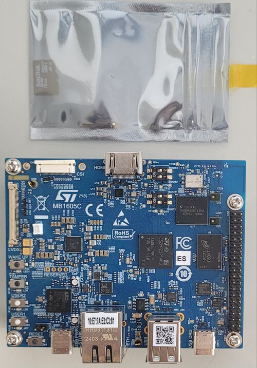
The STM32MP257x-DKx Discovery kit package (STM32MP257F-DK ![]() ) contains the items listed below.
) contains the items listed below.
| Position | Description |
|---|---|
| 1 | MB1605 motherboard |
| 2 | microSD™ card |
| LVDS displays and CSI cameras are available for purchase to complete this basic setup. |
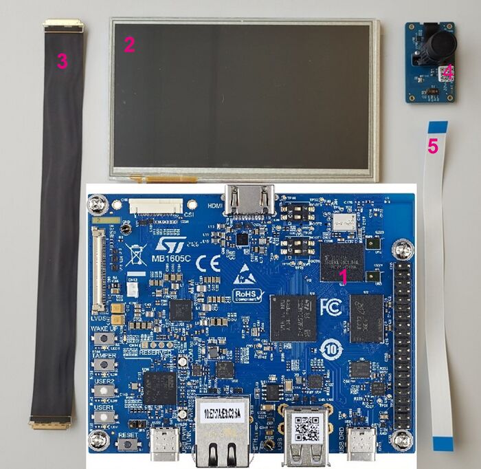
The complete set contains:
| Position | Description |
|---|---|
| 1 | MB1605 main board |
| 2 | MicroSD card |
| 3 | LVDS display cable (provided via B-LVDS7-WSVGA package) (optional) |
| 4 | 7” LVDS WSVGA display with EDT ETML0700Z9NDHA panel touch panel provided with the B-LVDS7-WSVGA package (optional) |
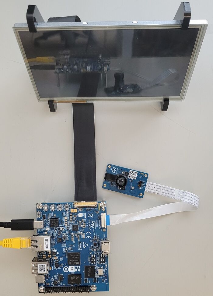
| 5 | Camera board FFC (provided with the B-CAMS-IMX package) (optional) |
| 6 | MB1854 board AI camera provided with the B-CAMS-IMX package (optional) |
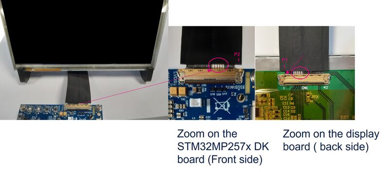
2.1. Connecting the LVDS display to the board (optional)[edit | edit source]
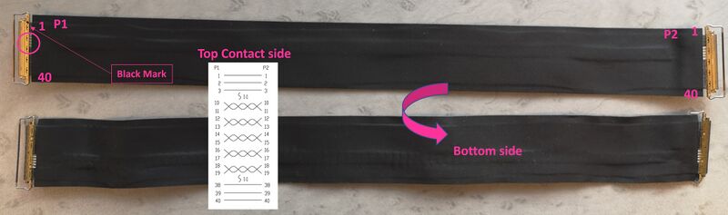
- Check the cable orientation shown above using the black mark and the white twisted pairs.
- Find the LVDS ports on the STM32MP257x-DK Discovery kit (CN2) and the display (CN1). The LVDS display box contains one cable.
- Insert the cable into each port as shown below:
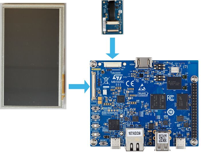
2.2. Connecting the MB1854 camera board to the board (optional)[edit | edit source]
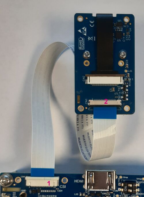
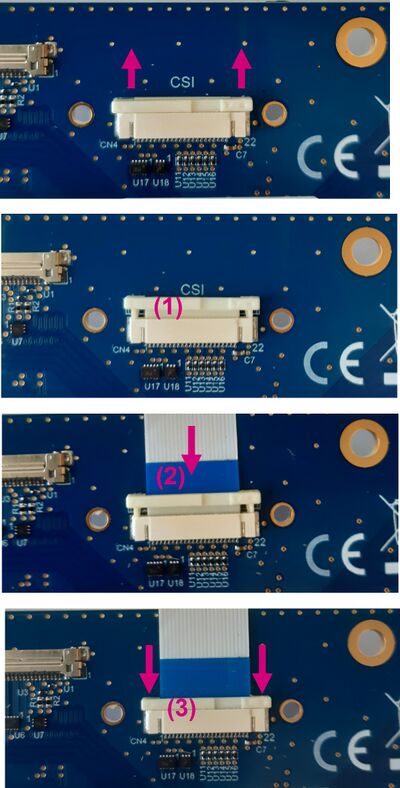
- Find the camera ports on the STM32MP257x-DK Discovery kit (CN8) (#1 in the image above) and MB1854 (CN1) (#2 in the image above). The camera box contains one FFC.
- For each port:
- Pull the black plastic (#1 in the image below) lightly to insert the contact side of the FFC towards the board (#2 in the image below).
- Push the black plastic carefully to hold the FFC (#3 in the image below).
2.3. STM32MP257x-DK Discovery kit assembled[edit | edit source]
3. Board overview[edit | edit source]
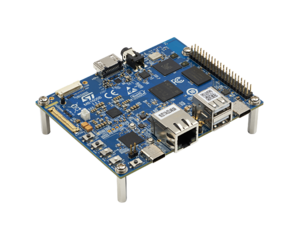
Main board MB1605, revision C-01: part of the STM32MP257x-DK Discovery kit ![]() .
.
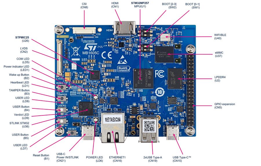
Details about the LEDs:
- LD11 turns green when a power connection is established (the power cable is inserted into the CN21 connector).
- Two general-purpose color LEDs (LED1 and LD9) are available as light indicators:
- The blue LED (LED1) is used as the Linux® Heartbeat LED, which blinks as long as Linux® is running on the Arm® Cortex®-A.
- The orange LED (LD9) is used as an STM32Cube example verdict LED.
- The two LEDs, LD7 (red) and LD8 (green), are free user LEDs that can be by configured by the user for any purpose, as explained in the LEDs and buttons on STM32 MPU boards wiki article.
- The LD5 and LD6 LEDs are used as an ST-LINK status indicator.
4. Board connection[edit | edit source]
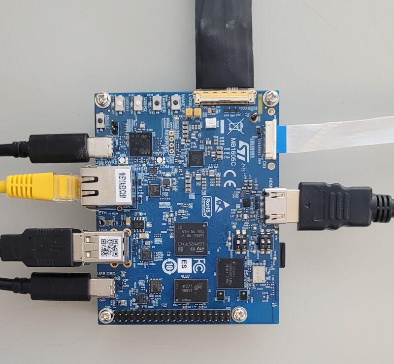
The image below shows the recommended connections for getting started with the STM32MP257x-DK Discovery kits. As shown in the board overview, other connectors are available for this board (for example, the GPIO expansion connector).
5. Boot switches[edit | edit source]
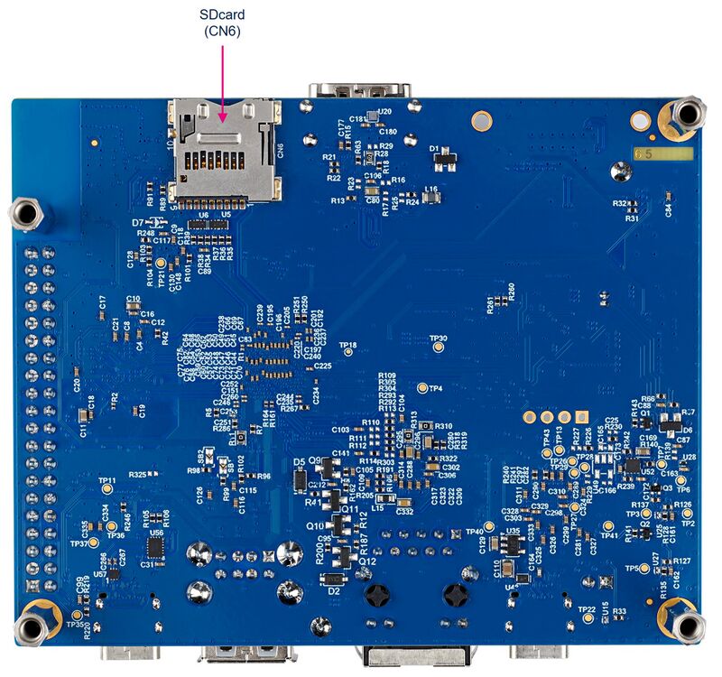
The STM32MP257x-DK Discovery kit can boot from different flash memory devices (microSD, eMMC) based on ROM code selection; using the microSD card is recommended.
| TD flavor | Boot 0 | Boot 1 | Boot 2 | Boot 3 | The boot-related switches (SW1 and SW2 in the board overview picture |
Storage device used for the Cortex-A35 boot | Storage device used for the Cortex-M33 boot |
|---|---|---|---|---|---|---|---|
| For any TD flavor (A35-TD or M33-TD) |
0 | 0 | 0 | 0 | USB/UART for programming | NA | |
| 1 | 1 | 0 | 0 | Development boot | NA | ||
| A35-TD flavor |
1 | 0 | 0 | 0 | SD card | NA | |
| 0 | 1 | 0 | 0 | eMMC | NA | ||
| M33-TD flavor |
1 | 1 | 1 | 0 | | | SD card | SD card |
| 0 | 0 | 0 | 1 | eMMC | eMMC |


When the switch is set to the "ON" position, the BOOTx value is "1"; otherwise it is "0".
6. GPIO mapping[edit | edit source]
6.1. GPIO expansion connector[edit | edit source]
The table below describes the pins of the GPIO expansion connector (CN5 in the board overview picture):
| Function | STM32 pin | Pin | Pin | STM32 pin | Function |
|---|---|---|---|---|---|
| 3V3 | - | 1 | 2 | - | 5V |
| GPIO2 / I2C8_SDA | PZ3 | 3 | 4 | - | 5V |
| GPIO3 / I2C8_SDL | PZ4 | 5 | 6 | - | GND |
| GPIO4 / MCO1 | PF11 | 7 | 8 | PF13 | GPIO14 / USART6_TX |
| GND | - | 9 | 10 | PF14 | GPIO15 / USART6_RX |
| GPIO17 / USART6_RTS | PG5 | 11 | 12 | PD2 | GPIO18 / SAI4_SCKA |
| GPIO27 | PZ9 | 13 | 14 | - | GND |
| GPIO22 | PZ0 | 15 | 16 | PZ1 | GPIO23 |
| 3V3 | - | 17 | 18 | PZ6 | GPIO24 |
| GPIO10 / SPI6_MOSI | PC7 | 19 | 20 | - | GND |
| GPIO9 / SPI6_MISO | PC4 | 21 | 22 | PZ7 | GPIO25 |
| GPIO11 / SPI6_SCK | PF7 | 23 | 24 | PF4 | GPIO8 / SPI6_NSS |
| GND | - | 25 | 26 | PZ5 | GPIO7 |
| I2C2_SDA | PF0 | 27 | 28 | PF2 | I2C2_SCL |
| GPIO5 / TIM8_CH4 | PC10 | 29 | 30 | - | GND |
| GPIO6 / TIM5_CH1 | PH8 | 31 | 32 | PA5 | GPIO12 / TIM2_CH4 |
| GPIO13 / TIM4_CH2 | PA1 | 33 | 34 | - | GND |
| GPIO19 / SAI4_FSA | PD0 | 35 | 36 | PF15 | GPIO16 / USART6_CTS |
| GPIO26 | PZ8 | 37 | 38 | PD1 | GPIO20 / SAI4_SDA |
| GND | - | 39 | 40 | PB5 | GPIO21 / SAI4_SDB |
6.2. User buttons and LEDs[edit | edit source]
The tables below describe the GPIO assignments for the user buttons and LEDs. Refer to the LEDs and buttons on STM32 MPU boards article for more details.
GPIO for LEDs
| LED color and label | GPIO |
|---|---|
| Green LD8 | PH5 |
| Red LD7 | PH4 |
| Orange LD9 | PH6 |
| Blue LED1 | PH7 |
GPIO for user buttons
| Button | GPIO |
|---|---|
| USER1 | PC5 |
| USER2 | PC11 |
7. References[edit | edit source]
Arm® is a registered trademark of Arm Limited (or its subsidiaries) in the US and/or elsewhere. ![]()
Arm® is a registered trademark of Arm Limited (or its subsidiaries) in the US and/or elsewhere. ![]()