1. Article purpose[edit | edit source]
The purpose of this article is to explain how to configure the analog-to-digital converter ADC internal peripheral using the device tree mechanism, relying on the bindings documentation that is the description of the required and optional device-tree properties.
The peripheral can be assigned to different contexts/software components, depending on the final product needs. Refer to How to assign an internal peripheral to an execution context for guidelines on this configuration.
The device tree file to configure depends on the context/component to which the ADC peripheral is assigned:
- U-Boot (Boot time context): refer to U-Boot overview.
- Linux® OS (Runtime context): refer to the IIO framework.https://wiki.st.com/stm32mpu/wiki/I3C_overview#STM32_I-internal_peripheral_controllertors
2. DT bindings documentation[edit | edit source]
U-Boot, Linux® OS: STM32 ADC device tree bindings: Documentation/devicetree/bindings/iio/adc/st,stm32-adc.yaml
3. DT configuration[edit | edit source]
This hardware description is a combination of the STM32 microprocessor device tree files (.dtsi extension) and board device tree files (.dts extension). See the Device tree for an explanation of the device tree file split.
STM32CubeMX can be used to generate the board device tree. Refer to How to configure the DT using STM32CubeMX for more details.
3.1. DT configuration (STM32/SoC level)[edit | edit source]
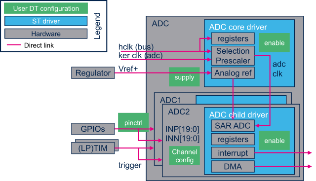
An ADC peripheral provides one or more ADCs. Some hardware common resources are managed in the ADC peripheral, whatever the number of ADC sub-blocks. In the following chapters, the ADC peripheral is called "ADC block", while "ADC" refers to an ADC peripheral sub-block.
The ADC DT nodes are structured as follows:
- The DT root node describes the ADC block parameters such as register areas, clocks and interrupts.
- The DT child nodes describe the ADCs independently.
3.1.1. STM32MP13x lines  [edit | edit source]
The ADC nodes are declared in stm32mp131.dtsi[1] and in stm32mp133.dtsi[2].
adc_1: adc@address {
	compatible = "st,stm32mp13-adc-core";
	...                                      /* common resources in 'adc_1' root node. */
	adc1: adc@0 {
		compatible = "st,stm32mp13-adc";
		...                              /* private resources in 'adc1' child node. */
	};
};
adc_2: adc@address {
	compatible = "st,stm32mp13-adc-core";
	...                                      /* common resources in 'adc_2' root node. */
	adc2: adc@0 {
		compatible = "st,stm32mp13-adc";
		...                              /* private resources in 'adc2' child node. */
	};
};
3.1.2. STM32MP15x lines [edit | edit source]
The ADC nodes are declared in stm32mp151.dtsi[3].
adc: adc@address {
	compatible = "st,stm32mp1-adc-core";
	...                                      /* common resources in 'adc' root node. */
	adc1: adc@0 {
		compatible = "st,stm32mp1-adc";
		...                              /* private resources in 'adc1' child node. */
	};
	adc2: adc@100 {
		compatible = "st,stm32mp1-adc";
		...                              /* private resources in 'adc2' child node. */
	};
};
3.1.3. STM32MP21x lines [edit | edit source]
The ADC nodes are declared in stm32mp211.dtsi[4].
adc_1: adc@404e0000 {
	compatible = "st,stm32mp21-adc-core";
	...                                      /* common resources in 'adc_1' root node. */
	adc1: adc@0 {
		compatible = "st,stm32mp21-adc";
		...                              /* private resources in 'adc1' child node. */
	};
};
adc_2: adc@404f0000 {
	compatible = "st,stm32mp21-adc-core";
	...                                      /* common resources in 'adc_2' root node. */
	adc2: adc@0 {
		compatible = "st,stm32mp21-adc";
		...                              /* private resources in 'adc2' child node. */
	};
};
3.1.4. STM32MP23x lines [edit | edit source]
The ADC nodes are declared in stm32mp231.dtsi[5].
adc_12: adc@404e0000 {
	compatible = "st,stm32mp23-adc-core";
	...                                      /* common resources in 'adc_12' root node. */
	adc1: adc@0 {
		compatible = "st,stm32mp23-adc";
		...                              /* private resources in 'adc1' child node. */
	};
	adc2: adc@100 {
		compatible = "st,stm32mp23-adc";
		...                              /* private resources in 'adc2' child node. */
	};
};
adc_3: adc@404f0000 {
	compatible = "st,stm32mp23-adc-core";
	...                                      /* common resources in 'adc_3' root node. */
	adc3: adc@0 {
		compatible = "st,stm32mp23-adc";
		...                              /* private resources in 'adc3' child node. */
	};
};
3.1.5. STM32MP25x lines [edit | edit source]
The ADC nodes are declared in stm32mp251.dtsi[6].
adc_12: adc@404e0000 {
	compatible = "st,stm32mp25-adc-core";
	...                                      /* common resources in 'adc_12' root node. */
	adc1: adc@0 {
		compatible = "st,stm32mp25-adc";
		...                              /* private resources in 'adc1' child node. */
	};
	adc2: adc@100 {
		compatible = "st,stm32mp25-adc";
		...                              /* private resources in 'adc2' child node. */
	};
};
adc_3: adc@404f0000 {
	compatible = "st,stm32mp25-adc-core";
	...                                      /* common resources in 'adc_3' root node. */
	adc3: adc@0 {
		compatible = "st,stm32mp25-adc";
		...                              /* private resources in 'adc3' child node. */
	};
};
3.2. DT configuration (board level)[edit | edit source]
The objective of this chapter is to explain how to enable and configure the ADC DT nodes for a board.
Peripheral configuration should be done in specific board device tree files (board dts file and pinctrl dtsi file).
3.2.1. Common resources for all ADCs[edit | edit source]
The DT root node must be filled in:
- Enable the ADC block by setting status = "okay".
- Configure the pins in use via pinctrl, through pinctrl-0 and pinctrl-names.
- Configure the analog supply voltage regulator[7] by setting vdda-supply = <&your_vdda_regulator>.
- Configure the analog reference voltage regulator[7] by setting vref-supply = <&your_vref_regulator>.
| The ADC block can use the internal VREFBUF[8] or any other external regulator[7] wired to VREF+ pin. |
3.2.2. Resources dedicated to an ADC[edit | edit source]
The DT child nodes ('adc<n=1, 2, 3>') must be filled in with the ADC and channels properties. The number <n> of ADC instances may vary depending on the STM32 Arm® Cortex® MPUs ![]() used, as described in ADC internal peripheral.
used, as described in ADC internal peripheral.
3.2.2.1. ADC properties[edit | edit source]
- Enable ADC by setting status = "okay".
- Set ADC resolution by setting assigned-resolution-bits = <12> (optional).
3.2.2.2. Channel properties[edit | edit source]
Each channel is described by a dedicated DT sub node, filled in with properties documented in Generic IIO bindings for ADC channels[9].
- Define channel index 'x' by setting reg = <x>.
- Enable differential channel pair (<vinp vinn>) by setting diff-channels = <x y> (optional).
Refer to the connectivity section of the ADC chapter in the reference manual, to determine the relevant pin indexes (x,y). The "x" index corresponds to the positive input INPx. For the negative input INNx, the index "y" of the associated positive input pin INPy, must be provided. An example of differential pins configuration is given in the DT configuration examples chapter below.
- Set the minimum sampling time [10] by setting st,min-sample-time-ns = <10000> (optional)
- Identifiy the channel by setting its name with label = "xxx" (optional).
Reserved labels allow to identify the internal channels.- "vrefint", "vddcore", "vddcpu", "vddq_ddr", "vddgpu": These internal channels are defined in the SoC DT. They can be removed in the board DT if they are not used.
- "vbat": This internal channel can be defined in the board DT. It is not defined by default in the SoC DT to save current consumption.
| Internal channels availability depends on the ADC instance used. It also depends on the STM32 microprocessor device. |
3.3. DT configuration examples[edit | edit source]
The example below shows how to configure ADC1 on STM32MP15x lines ![]() . Same applies for all STM32 Arm® Cortex® MPUs
. Same applies for all STM32 Arm® Cortex® MPUs ![]() :
:
- Input pin: use Pinctrl device tree configuration to configure PF12 as analog input.
- Analog supply: it is provided by one of the PMIC LDO regulators.
- Voltage reference: it is provided by the VREFBUF internal regulator.
- Input channel: configure ADC1_IN6 (e.g on PF12).
- Sampling time: the minimum sampling time is 10 µs.
# part of pin-controller dt node
adc1_in6_pins_a: adc1-in6 {
	pins {
		pinmux = <STM32_PINMUX('F', 12, ANALOG)>; /* configure 'PF12' as ANALOG */
	};
};
| ANA0 and ANA1 pins are dedicated to the ADC, so pinctrl definition is not needed for those pins. |
&adc {
	/* ADC block common resources */
	pinctrl-names = "default";
	pinctrl-0 = <&adc1_in6_pins_a>;              /* Use PF12 pin as ANALOG */
	vdda-supply = <&vdda>;                       /* Example to supply vdda pin by using a PMIC regulator
	vref-supply = <&vrefbuf>;                    /* Example to use VREFBUF (It needs to be enabled as well) */
	status = "okay";                             /* Enable ADC block */
	adc1: adc@0 {
	        #address-cells = <1>;
        	#size-cells = <0>;
		/* private resources for ADC1 */
		status = "okay";                     /* Enable ADC1 */
 		/* Single-ended channel */
		channel@6 {
			reg = <6>;               /* ADC1 in6 channel is used */
			st,min-sample-time-ns = <10000>;  /* 10µs sampling time */
		};
 		/* Configure channel 1 as differential (ANA1 - ANA0) */
		channel@1 {
			reg = <1>;               /* ADC1 inp1 and inn1 (inn1 equivalent to inp0) channels are used */
			diff-channels = <1 0>;
			st,min-sample-time-ns = <10000>;  /* 10µs sampling time */
		};
	};
};
4. How to configure the DT using STM32CubeMX[edit | edit source]
The STM32CubeMX tool can be used to configure the STM32MPU device and get the corresponding platform configuration device tree files.
STM32CubeMX may not support all the properties described in DT binding files listed in the above DT bindings documentation paragraph. If so, the tool inserts user sections in the generated device tree. These sections can then be edited to add some properties, and they are preserved from one generation to another. Refer to STM32CubeMX user manual for further information.
5. References[edit | edit source]
For additional information, refer to the following links:
- ↑ STM32MP131 device tree file
- ↑ STM32MP133 device tree file
- ↑ STM32MP151 device tree file
- ↑ STM32MP211 device tree file
- ↑ STM32MP231 device tree file
- ↑ STM32MP251 device tree file
- ↑ 7.0 7.1 7.2 Regulator overview
- ↑ VREFBUF internal peripheral
- ↑ Documentation/devicetree/bindings/iio/adc/adc.yaml , Generic IIO bindings for ADC channels
- ↑ How to get the best ADC accuracy in STM32, by STMicroelectronics
Arm® is a registered trademark of Arm Limited (or its subsidiaries) in the US and/or elsewhere. ![]()
Arm® is a registered trademark of Arm Limited (or its subsidiaries) in the US and/or elsewhere. ![]()