This article describes how the STM32 MPU Embedded Software distribution maps the various software memory needs in internal and external volatile memories.
1. Overview[edit | edit source]
This article shows the default memory mapping defined by STMicroelectronics in STM32MPU Embedded Software. It uses a subset of all memory regions that are exposed at hardware level: customers may use other memory regions or aliases that are not shown here but are described in the STM32 MPU reference manuals.
The objective of the default STM32MPU Embedded Software memory mapping is to propose a generic memory mapping that:
- allows demonstrating all the features proposed by the hardware platform and associated software.
- is compliant with the official ST boards.
2. Memory mapping[edit | edit source]
2.1. Overall memory mapping[edit | edit source]
The following figure shows assignment of the different memories to the different execution contexts.
The different memory aliases required by Cortex-M33 Armv8-M architecture to differentiate secure and nonsecure memories are not represented in below figure.
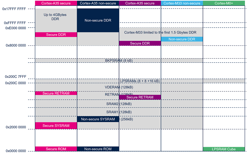
(*) LPSRAM only available on STM32MP25x lines ![]()
(**) CM0+ only available on STM32MP25x lines ![]()
3. Internal RAM mapping[edit | edit source]
SYSRAM, SRAMs, RETRAM, VDERAM and LPSRAM internal RAMs are mapped several times at different aliases in the memory map:
For SYSRAM, SRAMs, RETRAM and VDERAM possible aliases are: 0x0A0. ...., 0x0E0. ...., 0x20.. .... and 0x30.. .....
For LPSRAM possible aliases are: 0x200C0000 and 0x300C0000.
3.1. Overview[edit | edit source]
The SYSRAM, RETRAM, SRAM1/2, and VDERAM (if Video decoder and Video encoder are not used) can be assigned to different execution contexts of the platform by configuring the [RISAB internal peripheral|RISAB]] memory firewall.
The STM32MPU Embedded Software is based on a default internal RAM memory mapping which can be modified by customer to fit with its product requirements. The next chapters describe the constraints per type of RAM and memory region.
3.1.1. SYSRAM[edit | edit source]
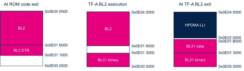
The following figure shows the evolution of the SYSRAM mapping during boot flow.
At runtime, the SYSRAM is split in two regions:
- 128kB Cortex-A35 Secure region dedicated to TF-A BL31 secure monitor.
- 128kB Cortex-A35 nonsecure region dedicated to HPDMA linked lists management.
See SYSRAM internal memory for more information.
3.1.2. SRAM1 and SRAM2[edit | edit source]
In A35-TD flavor ![]() :
:
SRAM1 is used by FSBL TF-A BL2 to store DDR controller firmware and prepare OTP shadow.
At runtime, the first 4kByte of the SRAM1 are reserved for OTP shadow allowing to share OTP between Cortex-A35 OP-TEE secure OS and Cortex-M33 TF-M secure OS.
Rest of SRAM1 and SRAM2 are allocated in STM32MPU Embedded Software to Cortex-M33 secure and nonsecure firmware, when not located in DDR for some low power or performance reasons.
The following figure shows the evolution of SRAM mapping during boot flow:
In M33-TD flavor ![]() :
:
SRAM is used during MCUboot execution:
- SRAM1 to host the MCUboot memory stack (~46KB).
- SRAM2 to host DDR buffer needed to load the firmware from the mass storage (~35KB).
At runtime :
- SRAM1 is used to manage exchanges between both cores:
- A dedicated mirror is used to share the BSEC non secret OTP that are necessary for both cores to configure the platform. The area is a non-secure area that can be accessible by all cores but limited as read only partition.
- SCMI CID1 buffer to exchange messages between the CID1 clients (secure, non-secure) and the server.
- PSA buffer to exchange between client and the CID2 server.
- A TFM_SHARED_DATA area to exchange data between MCUboot and TF-M.
- CM33_SRAM1 as reserved area for default M33 usage (rest of the memory).
- SRAM1 is used to manage exchanges between both cores:
- SRAM2 is used as a free internal ram buffer that can be used by the M33 non secure application.

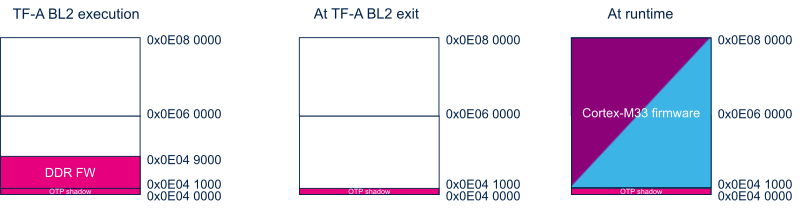
3.1.3. RETRAM[edit | edit source]
In STM32MPU Embedded Software, RETRAM is used for:
A35-TD flavor ![]() :
:
- DDR parameters saving to restore DDR access on low power modes exit.
- Cortex-M33 firmware that must be preserved in low power Standby mode. It is mainly the low power entry and exit functions executed by the Cortex-M33 secure context.

In M33-TD flavor ![]()
The following figure shows the evolution of the RETRAM mapping during boot flow.
- ROM code loads MCUboot from storage device to RETRAM for his execution.
- After MCUboot execution, RETRAM is used to manage the low power restoration firmware (including RIF and DDR parameters).

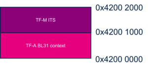
3.1.4. BKPSRAM[edit | edit source]
In STM32MPU Embedded Software, the BKPSRAM is used as following:
- 4kB dedicated to secure SW components context saving for restoration during low power exit sequence.
- 4kB for TF-M Internal Trusted Storage (ITS).
3.1.5. VDERAM[edit | edit source]
In STM32MPU Embedded Software, VDERAM is by default allocated to hardware video encoder and decoder if VENC or VDEC is assigned to one execution context.
Else if none is used, VDERAM could be allocated to any execution context.
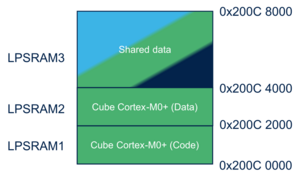
3.1.6. LPSRAM (only on STM32MP25x lines  )[edit | edit source]
LPSRAM are dedicated to Cortex-M0+ firmware and associated shared memory. The default memory mapping is the following one:
4. DDR mapping[edit | edit source]
STM32MPU Embedded Software proposes a generic DDR mapping compliant with DDR from 256MByte to 4GByte, allowing to demonstrate all STM32MPU Embedded Software features.
The first 64MByte are reserved to firmware:
- Cortex-M33 secure OS (TF-M code and data)
- Cortex-M33 nonsecure application (Cube code and data)
- Cortex-A35 secure OS (OP-TEE)
- Shared memory IPC between Cortex-A35 and Cortex-M33
- Cortex-M33 LTDC layer (only for M33-TD flavor
 )
)
Rest of the DDR is allocated to the Linux kernel and applications.
All bus master peripherals can access only to the lower 2GByte of DDR as they are 32bit capable. Linux CMA and reserved memories used for contiguous buffers allocation must be defined in the first 2GByte of DDR.
In case of generic memory allocation done in the higher 2GByte of DDR, Linux kernel offers SWIOTLB mechanism to recopy data in a bounce buffer located in the lower 2GByte of DDR compliant with 32bit bus master peripherals.
The following figure shows the evolution of the DDR mapping during the boot sequence.
A35-TD flavor ![]() :
:
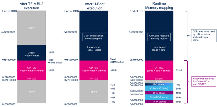
M33-TD flavor ![]() :
:

Note:
|
It is customer responsibility to adapt DDR mapping to its product configuration (DDR size and SW components)
4.1. How to configure RAM mapping[edit | edit source]
The memory mapping is defined in each SW component device tree file using Reserved_memory bindings. Customer can change name, based address, size, and access rights of each region according to its product needs.
To ensure the consistency of the system, memory declarations of each SW component have to be updated according to the expected configuration.
ST recommands using STM32CubeMX tools to generate coherent memory mapping with associated access rights.
Arm® is a registered trademark of Arm Limited (or its subsidiaries) in the US and/or elsewhere. ![]()