Registered User mNo edit summary |
Registered User mNo edit summary Tag: 2017 source edit |
||
| (12 intermediate revisions by 2 users not shown) | |||
| Line 1: | Line 1: | ||
{{ApplicableFor | |||
{{ | |MPUs list=STM32MP15x | ||
|MPUs checklist=STM32MP13x, STM32MP15x, STM32MP21x, STM32MP23x, STM32MP25x | |||
}} | |||
This article provides an overview of STM32MP157x-EV1 Evaluation boards. | |||
==Article purpose== | ==Article purpose== | ||
This article briefly describes: | |||
* How to assemble together the different elements provided in the commercial box | * How to assemble together the different elements provided in the commercial box | ||
* What are the different components present on the boards | * What are the different components present on the boards | ||
| Line 16: | Line 14: | ||
* What are the configurations of the connectors pins | * What are the configurations of the connectors pins | ||
This article is valid | This article is valid for the {{Board | type=157A-EV1 | name=short}}<ref>[https://www.st.com/en/evaluation-tools/stm32mp157a-ev1.html STM32MP157A-EV1 - Evaluation board with STM32MP157A MPU]</ref>, {{Board | type=157D-EV1 | name=short}}<ref>[https://www.st.com/en/evaluation-tools/stm32mp157d-ev1.html STM32MP157D-EV1 - Evaluation board with STM32MP157D MPU]</ref>, {{Board | type=157C-EV1 | name=short}}<ref>[https://www.st.com/en/evaluation-tools/stm32mp157c-ev1.html STM32MP157C-EV1 - Evaluation board with STM32MP157C MPU]</ref> and {{Board | type=157F-EV1 | name=short}}<ref>[https://www.st.com/en/evaluation-tools/stm32mp157f-ev1.html STM32MP157F-EV1 - Evaluation board with STM32MP157F MPU]</ref> Evaluation boards: the part numbers are specified in the [[STM32MP15 microprocessor#Part number codification|STM32MP15 microprocessor part numbers]] article. | ||
{{Warning|This article is only an introduction to the STM32MP157x-EV1 Evaluation board. Detailed information can be found in the [[STM32MP15 resources# | {{Warning|This article is only an introduction to the STM32MP157x-EV1 Evaluation board. Detailed information can be found in the [[STM32MP15 resources#Boards user manuals|'''STM32MP157x-EV1 Evaluation boards user manuals''']].}} | ||
==Board assembly== | ==Board assembly== | ||
{{: | {{:STM32MP157x-EV1 - board assembly}} | ||
==Board overview== | ==Board overview== | ||
{| | {| class="st-table" | ||
|+ | |+ | ||
! Position !! Description | ! Position !! Description | ||
| Line 38: | Line 36: | ||
|} | |} | ||
{| | {| class="st-table" | ||
|+ | |+ | ||
! Position !! Description !! Position !! Description | ! Position !! Description !! Position !! Description | ||
| Line 54: | Line 52: | ||
|| 17 (<span id{{=}}"MB1262-U5">'''U5'''</span>) || SmartCard (back side slot) | || 17 (<span id{{=}}"MB1262-U5">'''U5'''</span>) || SmartCard (back side slot) | ||
|- | |- | ||
| 18 (<span id{{=}}"MB1262-LD1">'''LD1'''</span>) || Ethernet LED (green)<ref>LD1 (MB1262): flashes green when Ethernet connection established</ref> | | 18 (<span id{{=}}"MB1262-LD1">'''LD1'''</span>) || Ethernet LED (green)<ref group="LEDs">LD1 (MB1262): flashes green when Ethernet connection established</ref> | ||
|| 19 (<span id{{=}}"MB1262-CN6">'''CN6'''</span>) || Ethernet daughterboard connector | || 19 (<span id{{=}}"MB1262-CN6">'''CN6'''</span>) || Ethernet daughterboard connector | ||
|- | |- | ||
| Line 64: | Line 62: | ||
|- | |- | ||
| 24 (<span id{{=}}"MB1262-CN16">'''CN16'''</span>) || USB micro-AB (OTG) | | 24 (<span id{{=}}"MB1262-CN16">'''CN16'''</span>) || USB micro-AB (OTG) | ||
|| 25 (<span id{{=}}"MB1262-LD2">'''LD2'''</span>) || USB OTG LED (green)<ref>LD2 (MB1262): turns green when USB OTG connection established</ref> | || 25 (<span id{{=}}"MB1262-LD2">'''LD2'''</span>) || USB OTG LED (green)<ref group="LEDs">LD2 (MB1262): turns green when USB OTG connection established</ref> | ||
|- | |- | ||
| 26 (<span id{{=}}"MB1262-LD2">'''LD3'''</span>) || USB Type-A LED (red)<ref>LD3 (MB1262): turns red if USB Type-A connection established</ref> | | 26 (<span id{{=}}"MB1262-LD2">'''LD3'''</span>) || USB Type-A LED (red)<ref group="LEDs">LD3 (MB1262): turns red if USB Type-A connection established</ref> | ||
|| 27 (<span id{{=}}"MB1262-CN17">'''CN17'''</span>) || MFX header 4 pins | || 27 (<span id{{=}}"MB1262-CN17">'''CN17'''</span>) || MFX header 4 pins | ||
|- | |- | ||
| Line 84: | Line 82: | ||
[[File: STM32MP157x-EV1_front_side.jpg | thumb | 800px | left | link= | STM32MP157x-EV1 Evaluation board front side <br> '''STM32MP157A-EV1''' shown here (picture is not contractual)]] | [[File: STM32MP157x-EV1_front_side.jpg | thumb | 800px | left | link= | STM32MP157x-EV1 Evaluation board front side <br> '''STM32MP157A-EV1''' shown here (picture is not contractual)]] | ||
{| | {| class="st-table" | ||
|+ | |+ | ||
! Position !! Description !! Position !! Description | ! Position !! Description !! Position !! Description | ||
|- | |- | ||
| 50 (<span id{{=}}"MB1263-B1">'''B1'''</span>) || Reset button | | 50 (<span id{{=}}"MB1263-B1">'''B1'''</span>) || Reset button | ||
|| 51 (<span id{{=}}"MB1263-LD2">'''LD2'''</span>) || User LED (red)<ref name="User LEDs">LD2, LD3, LD4, LD5 (MB1263): some user LEDs are used to reflect the system activity, while the others are left free to be used by the application, as explained in [[LEDs and buttons on STM32 MPU boards]] article</ref> | || 51 (<span id{{=}}"MB1263-LD2">'''LD2'''</span>) || User LED (red)<ref group="LEDs" name="User LEDs">LD2, LD3, LD4, LD5 (MB1263): some user LEDs are used to reflect the system activity, while the others are left free to be used by the application, as explained in [[LEDs and buttons on STM32 MPU boards]] article</ref> | ||
|- | |- | ||
| 52 (<span id{{=}}"MB1263-B2">'''B2'''</span>) || User button (PA13) | | 52 (<span id{{=}}"MB1263-B2">'''B2'''</span>) || User button (PA13) | ||
|| 53 (<span id{{=}}"MB1263-LD3">'''LD3'''</span>) || User LED (green | || 53 (<span id{{=}}"MB1263-LD3">'''LD3'''</span>) || User LED (green)<ref group="LEDs" name="User LEDs"/> | ||
|- | |- | ||
| 54 (<span id{{=}}"MB1263-B3">'''B3'''</span>) || User button (PA14) | | 54 (<span id{{=}}"MB1263-B3">'''B3'''</span>) || User button (PA14) | ||
|| 55 (<span id{{=}}"MB1263-LD5">'''LD5'''</span>) || User LED (blue | || 55 (<span id{{=}}"MB1263-LD5">'''LD5'''</span>) || User LED (blue)<ref group="LEDs" name="User LEDs"/> | ||
|- | |- | ||
| 56 (<span id{{=}}"MB1263-LD4">'''LD4'''</span>) || User LED (orange | | 56 (<span id{{=}}"MB1263-LD4">'''LD4'''</span>) || User LED (orange)<ref group="LEDs" name="User LEDs"/> | ||
|| 57 (<span id{{=}}"MB1263-B4">'''B4'''</span>) || Wakeup button | || 57 (<span id{{=}}"MB1263-B4">'''B4'''</span>) || Wakeup button | ||
|- | |- | ||
| 58 (<span id{{=}}"MB1263-LD1">'''LD1'''</span>) || Power LED (green)<ref>LD1 (MB1263): turns green if power connection established</ref> | | 58 (<span id{{=}}"MB1263-LD1">'''LD1'''</span>) || Power LED (green)<ref group="LEDs">LD1 (MB1263): turns green if power connection established</ref> | ||
|| 59 (<span id{{=}}"MB1263-CN1">'''CN1'''</span>) || MB1263 power 5V-3A | || 59 (<span id{{=}}"MB1263-CN1">'''CN1'''</span>) || MB1263 power 5V-3A | ||
|- | |- | ||
| Line 106: | Line 104: | ||
|| 61 (<span id{{=}}"MB1263-U3">'''U3'''</span>) || PMIC (STPMIC1A) | || 61 (<span id{{=}}"MB1263-U3">'''U3'''</span>) || PMIC (STPMIC1A) | ||
|- | |- | ||
| 62 (<span id{{=}}"MB1263-LD6">'''LD6'''</span>) || ST-LINK/V2-1 LED (bicolor)<ref>LD6 (MB1263): flashes red if ST-LINK/V2-1 connection not established, else green</ref> | | 62 (<span id{{=}}"MB1263-LD6">'''LD6'''</span>) || ST-LINK/V2-1 LED (bicolor)<ref group="LEDs">LD6 (MB1263): flashes red if ST-LINK/V2-1 connection not established, else green</ref> | ||
|| 63 (<span id{{=}}"MB1263-CN4">'''CN4'''</span>) || USB micro-B (ST-LINK/V2-1) | || 63 (<span id{{=}}"MB1263-CN4">'''CN4'''</span>) || USB micro-B (ST-LINK/V2-1) | ||
|- | |- | ||
| Line 116: | Line 114: | ||
|} | |} | ||
<br clear=all> | <br clear=all> | ||
Details about some LEDs: | Details about some LEDs: | ||
<references /> | <references group="LEDs"/> | ||
==Board connection== | ==Board connection== | ||
The connections shown in the picture below are the ones recommended to start with the STM32MP157x-EV1 Evaluation boards. As shown in the [[#Board overview|board overview]], other connectors are available for this board (for example CAN). | The connections shown in the picture below are the ones recommended to start with the STM32MP157x-EV1 Evaluation boards. As shown in the [[#Board overview|board overview]], other connectors are available for this board (for example CAN). | ||
{{: | {{:STM32MP157x-EV1 - board connections}} | ||
==Switches and jumpers== | ==Switches and jumpers== | ||
| Line 137: | Line 134: | ||
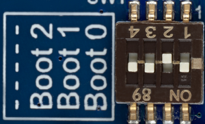
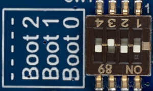
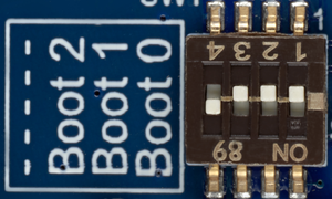
===Boot related switches=== | ===Boot related switches=== | ||
The STM32MP157x-EV1 Evaluation boards can boot from different Flash devices (microSD, eMMC...); using the microSD card is recommended. | The STM32MP157x-EV1 Evaluation boards can boot from different Flash devices (microSD, eMMC...); using the microSD card is recommended. | ||
{| | {| class="st-table" | ||
|+ Boot modes | |+ Boot modes | ||
! Boot mode !! Boot 2 !! Boot 1 !! Boot 0 | ! Boot mode !! Boot 2 !! Boot 1 !! Boot 0 | ||
| Line 155: | Line 152: | ||
The boot related switches ([[#MB1263-SW1|SW1]] on the board overview picture) must be configured as illustrated by one of the following pictures: | The boot related switches ([[#MB1263-SW1|SW1]] on the board overview picture) must be configured as illustrated by one of the following pictures: | ||
{| class=" | {| class="st-table" | ||
| [[File:STM32MP157x-EV1_boot_switches_engineering_mode.png|thumb|center|link=|Engineering boot]] || [[File:STM32MP157x-EV1_boot_switches_NOR.png|thumb|center|link=|Boot from NOR]] | | [[File:STM32MP157x-EV1_boot_switches_engineering_mode.png|thumb|center|link=|Engineering boot]] || [[File:STM32MP157x-EV1_boot_switches_NOR.png|thumb|center|link=|Boot from NOR]] | ||
|- | |- | ||
| Line 169: | Line 166: | ||
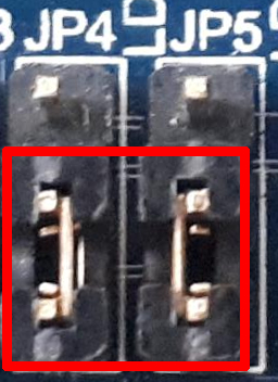
The connection is switched by setting JP4 and JP5 jumpers as shown in following pictures: | The connection is switched by setting JP4 and JP5 jumpers as shown in following pictures: | ||
{| class=" | {| class="st-table" | ||
| [[File:STM32MP157x-EV1_JP4_JP5_UART4_on_DB9_CN12.png|thumb|center|link=|UART4 is connected to the RS232, D-type, 9-pins [[#MB1262-CN12|CN12]] connector]] || [[File:STM32MP157x-EV1_JP4_JP5_UART4_on_ST-Link_V2-1_CN4.png|thumb|center|link=|UART4 is connected to the USB micro-B ST-LINK/V2-1 [[#MB1263-CN4|CN4]] connector]] | | [[File:STM32MP157x-EV1_JP4_JP5_UART4_on_DB9_CN12.png|thumb|center|link=|UART4 is connected to the RS232, D-type, 9-pins [[#MB1262-CN12|CN12]] connector]] || [[File:STM32MP157x-EV1_JP4_JP5_UART4_on_ST-Link_V2-1_CN4.png|thumb|center|link=|UART4 is connected to the USB micro-B ST-LINK/V2-1 [[#MB1263-CN4|CN4]] connector]] | ||
|} | |} | ||
| Line 177: | Line 174: | ||
===Motor control connector=== | ===Motor control connector=== | ||
The pins of the motor control connector ([[#MB1262-CN22|CN22]] on the board overview picture) are described in the following table.<br> | The pins of the motor control connector ([[#MB1262-CN22|CN22]] on the board overview picture) are described in the following table.<br> | ||
Due to the sharing of some IOs by multiple peripherals, '''the motor control interface is not enabled by default''', and the motor control cannot be operated simultaneously with the camera, audio codec, CAN and GPIO expansion (GPIO6, 7 and 12): more details (e.g. enabling the motor control interface) in the [[STM32MP15 resources# | Due to the sharing of some IOs by multiple peripherals, '''the motor control interface is not enabled by default''', and the motor control cannot be operated simultaneously with the camera, audio codec, CAN and GPIO expansion (GPIO6, 7 and 12): more details (e.g. enabling the motor control interface) in the [[STM32MP15 resources#Boards user manuals|'''STM32MP157x-EV1 Evaluation boards user manuals''']]. | ||
{{Warning | The pin 1 position (upper left) on this figure is the opposite compared to the board (bottom right)}} | {{Warning | The pin 1 position (upper left) on this figure is the opposite compared to the board (bottom right)}} | ||
{| style="text-align:center;" | {| class="st-table" style="text-align:center;" | ||
|+ Motor control connector | |+ Motor control connector | ||
! Description !! Function !! STM32 pin !! Pin !! Pin !! STM32 pin !! Function !! Description | ! Description !! Function !! STM32 pin !! Pin !! Pin !! STM32 pin !! Function !! Description | ||
| Line 223: | Line 220: | ||
The pins of the GPIO expansion connector ([[#MB1262-CN21|CN21]] on the board overview picture) are described in the following table: | The pins of the GPIO expansion connector ([[#MB1262-CN21|CN21]] on the board overview picture) are described in the following table: | ||
{{Warning | The pin 1 position (upper left) on this figure is the opposite compared to the board (bottom right)}} | {{Warning | The pin 1 position (upper left) on this figure is the opposite compared to the board (bottom right)}} | ||
{| style="text-align:center;" | {| class="st-table" style="text-align:center;" | ||
|+ GPIO expansion connector | |+ GPIO expansion connector | ||
! Function !! STM32 pin !! Pin !! Pin !! STM32 pin !! Function | ! Function !! STM32 pin !! Pin !! Pin !! STM32 pin !! Function | ||
| Line 229: | Line 226: | ||
| 3V3 || - || 1 || 2 || - || 5V | | 3V3 || - || 1 || 2 || - || 5V | ||
|- | |- | ||
| GPIO2 / I2C5_SDA< | | GPIO2 / I2C5_SDA<ref group="EX" name="I2C5">The I2C5 is shared between the I2C EXT connector and the GPIO expansion connector. By default, the I2C5 is connected to the I2C EXT connector thanks to Solder Bridges: more details in the [[STM32MP15 resources#Boards user manuals|STM32MP157x-EV1 Evaluation boards user manuals]].</ref> || PA12 || 3 || 4 || - || 5V | ||
|- | |- | ||
| GPIO3 / I2C5_SCL< | | GPIO3 / I2C5_SCL<ref group="EX" name="I2C5"/> || PA11 || 5 || 6 || - || GND | ||
|- | |- | ||
| GPIO4 / MCO1 || PI11 || 7 || 8 || PB10 || GPIO14 / USART3_TX | | GPIO4 / MCO1 || PI11 || 7 || 8 || PB10 || GPIO14 / USART3_TX | ||
| Line 237: | Line 234: | ||
| GND || - || 9 || 10 || PB12 || GPIO15 / USART3_RX | | GND || - || 9 || 10 || PB12 || GPIO15 / USART3_RX | ||
|- | |- | ||
| GPIO17 / USART3_RTS || PG8 || 11 || 12 || PI5 || GPIO18 / SAI2_SCKA< | | GPIO17 / USART3_RTS || PG8 || 11 || 12 || PI5 || GPIO18 / SAI2_SCKA <ref group="EX" name="SAI2 ">The SAI2 is shared between the audio codec and the GPIO expansion connector. By default, the SAI2 is connected to the audio codec thanks to Solder Bridges: more details in the [[STM32MP15 resources#Boards user manuals|STM32MP157x-EV1 Evaluation boards user manuals]].</ref> | ||
|- | |- | ||
| GPIO27 / SDMMC3_D3 || PD7 || 13 || 14 || - || GND | | GPIO27 / SDMMC3_D3 || PD7 || 13 || 14 || - || GND | ||
| Line 261: | Line 258: | ||
| GPIO13 / TIM8_CH4 || PI2 || 33 || 34 || - || GND | | GPIO13 / TIM8_CH4 || PI2 || 33 || 34 || - || GND | ||
|- | |- | ||
| GPIO19 / SAI2_FSA< | | GPIO19 / SAI2_FSA<ref group="EX" name="SAI2 "/> || PI7 || 35 || 36 || PI10 || GPIO16 / USART3_CTS | ||
|- | |- | ||
| GPIO26 / SDMMC3_D2 || PF5 || 37 || 38 || PI6 || GPIO20 / SAI2_SDA< | | GPIO26 / SDMMC3_D2 || PF5 || 37 || 38 || PI6 || GPIO20 / SAI2_SDA<ref group="EX" name="SAI2 "/> | ||
|- | |- | ||
| GND || - || 39 || 40 || PF11 || GPIO21 / SAI2_SDB< | | GND || - || 39 || 40 || PF11 || GPIO21 / SAI2_SDB<ref group="EX" name="SAI2 "/> | ||
|} | |} | ||
< | <references group="EX"/> | ||
===JTAG connector=== | ===JTAG connector=== | ||
The pins of the JTAG connector ([[#MB1262-CN14|CN14]] on the board overview picture) are described in the following table: | The pins of the JTAG connector ([[#MB1262-CN14|CN14]] on the board overview picture) are described in the following table: | ||
{| style="text-align:center;" | {| class="st-table" style="text-align:center;" | ||
|+ JTAG connector | |+ JTAG connector | ||
! Function !! Pin !! Pin !! Function | ! Function !! Pin !! Pin !! Function | ||
| Line 301: | Line 297: | ||
The GPIO assignments for the user buttons and LEDs are described in the following table. Refer to [[LEDs and buttons on STM32 MPU boards]] article to get information on the functional mapping for each one. | The GPIO assignments for the user buttons and LEDs are described in the following table. Refer to [[LEDs and buttons on STM32 MPU boards]] article to get information on the functional mapping for each one. | ||
{| style="text-align:center;" | {| class="st-table" style="text-align:center;" | ||
|+ GPIO for user buttons and LEDs | |+ GPIO for user buttons and LEDs | ||
! LED color and label | ! LED color and label | ||
| Line 307: | Line 303: | ||
! GPIO | ! GPIO | ||
|- | |- | ||
| | | <span style="color: green;">Green</span> LD3 (*) | ||
| USER1 (*) | | USER1 (*) | ||
| PA14 | | PA14 | ||
|- | |- | ||
| | | <span style="color: red;">Red</span> LD2 (*) | ||
| USER2 (*) | | USER2 (*) | ||
| PA13 | | PA13 | ||
|- | |- | ||
| | | <span style="color: orange;">Orange</span> LD4 | ||
| - | | - | ||
| PD8 | | PD8 | ||
|- | |- | ||
| | | <span style="color: blue;">Blue</span> LD5 | ||
| - | | - | ||
| PD9 | | PD9 | ||
| Line 325: | Line 321: | ||
{{Warning| (*) Both a LED and a button are connected to the same GPIO, with inverted logic for the LED control (so the LED is switched on when the GPIO output is set to low).}} | {{Warning| (*) Both a LED and a button are connected to the same GPIO, with inverted logic for the LED control (so the LED is switched on when the GPIO output is set to low).}} | ||
==References== | |||
<references/> | |||
<noinclude> | |||
{{ReviewsComments|File to be reviewed by the marketing communication team}} | |||
{{PublicationRequestId | 7663 | 2018-06-19 | AlainF}} | |||
[[Category:STM32MP15 Evaluation boards|00]] | |||
[[Category:ST boards]] | |||
</noinclude> | |||
Latest revision as of 11:36, 25 October 2024
This article provides an overview of STM32MP157x-EV1 Evaluation boards.
1. Article purpose[edit | edit source]
This article briefly describes:
- How to assemble together the different elements provided in the commercial box
- What are the different components present on the boards
- How to connect the boards to external material
- How to configure the board for boot
- How to select RS232 UART or ST-LINK/V2-1 connectors
- What are the configurations of the connectors pins
This article is valid for the STM32MP157A-EV1 ![]() [1], STM32MP157D-EV1
[1], STM32MP157D-EV1 ![]() [2], STM32MP157C-EV1
[2], STM32MP157C-EV1 ![]() [3] and STM32MP157F-EV1
[3] and STM32MP157F-EV1 ![]() [4] Evaluation boards: the part numbers are specified in the STM32MP15 microprocessor part numbers article.
[4] Evaluation boards: the part numbers are specified in the STM32MP15 microprocessor part numbers article.
2. Board assembly[edit | edit source]
The STM32MP157x-EV1 Evaluation boards packages (STM32MP157A-EV1 ![]() , STM32MP157D-EV1
, STM32MP157D-EV1 ![]() , STM32MP157C-EV1
, STM32MP157C-EV1 ![]() and STM32MP157F-EV1
and STM32MP157F-EV1 ![]() ) include all the items listed below.
) include all the items listed below.
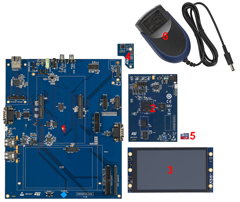
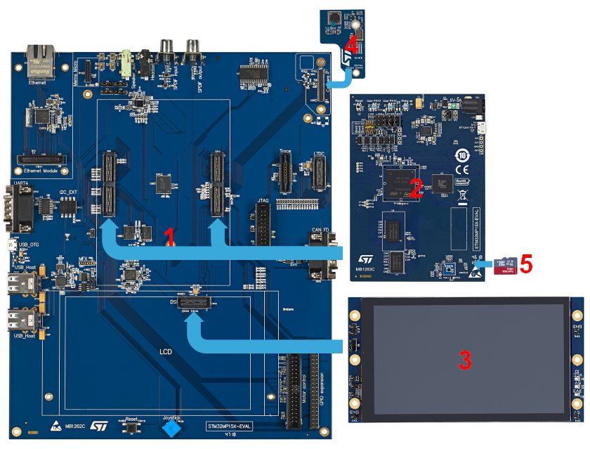
| Position | Description |
|---|---|
| 1 | MB1262 motherboard |
| 2 | MB1263 daughterboard |
| 3 | MB1230 DSI 720p display |
| 4 | MB1379 daughterboard camera (OmniVision OV5640 camera sensor) |
| 5 | microSD card |
| 6 | Power supply block (5V, 3A) |
The following figures explain how to assemble these different items to get the STM32MP157x-EV1 Evaluation boards.
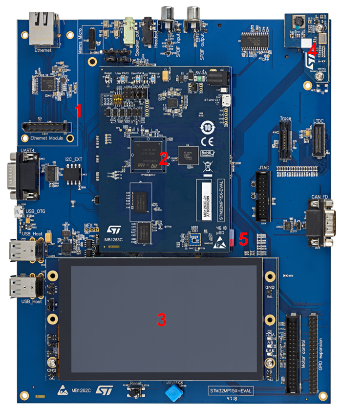
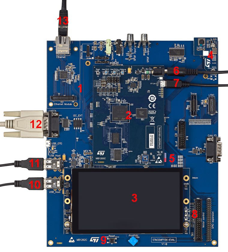
3. Board overview[edit | edit source]
| Position | Description |
|---|---|
| 1 | MB1262 motherboard |
| 2 | MB1263 daughterboard |
| 3 | MB1230 DSI 720p display |
| 4 (CN7) | MB1379 daughterboard camera |
| 5 | microSD card |
| Position | Description | Position | Description |
|---|---|---|---|
| 10 (CN3) | Ethernet | 11 (CN8) | Microphone MEMS daughterboard connector |
| 12 (CN4) | Speaker audio output | 13 (CN5) | Headset audio output |
| 14 (U8) | Audio codec (Wolfson WM8994) | 15 (CN1) | SPDIF RX (input) |
| 16 (CN2) | SPDIF TX (output) | 17 (U5) | SmartCard (back side slot) |
| 18 (LD1) | Ethernet LED (green)[LEDs 1] | 19 (CN6) | Ethernet daughterboard connector |
| 20 (U10) | Trace connector | 21 (CN11) | LTDC connector |
| 22 (CN12) | RS232 (UART4) | 23 (CN13) | External E2P connector |
| 24 (CN16) | USB micro-AB (OTG) | 25 (LD2) | USB OTG LED (green)[LEDs 2] |
| 26 (LD3) | USB Type-A LED (red)[LEDs 3] | 27 (CN17) | MFX header 4 pins |
| 28 (CN14) | JTAG connector | 29 (CN15) | CAN FD |
| 30 (CN18) | 2 USB Type-A (host) | 31 (CN20) | 2 USB Type-A (host) |
| 32 (B2) | Reset button | 33 (B1) | Joystick |
| 34 (CN22) | Motor control connector | 35 (CN21) | GPIO expansion connector |
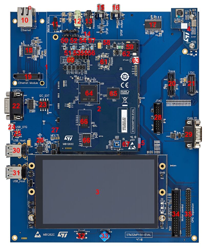
| Position | Description | Position | Description |
|---|---|---|---|
| 50 (B1) | Reset button | 51 (LD2) | User LED (red)[LEDs 4] |
| 52 (B2) | User button (PA13) | 53 (LD3) | User LED (green)[LEDs 4] |
| 54 (B3) | User button (PA14) | 55 (LD5) | User LED (blue)[LEDs 4] |
| 56 (LD4) | User LED (orange)[LEDs 4] | 57 (B4) | Wakeup button |
| 58 (LD1) | Power LED (green)[LEDs 5] | 59 (CN1) | MB1263 power 5V-3A |
| 60 (SW1) | Boot mode selection | 61 (U3) | PMIC (STPMIC1A) |
| 62 (LD6) | ST-LINK/V2-1 LED (bicolor)[LEDs 6] | 63 (CN4) | USB micro-B (ST-LINK/V2-1) |
| 64 (U4) | STM32MP157x 18x18 | 65 (U5) | eMMC |
| 66 (U6/U7) | 2 x DDR3L 16 bits | 67 (µSD) | microSD 3.0 card (back side slot) |
Details about some LEDs:
- ↑ LD1 (MB1262): flashes green when Ethernet connection established
- ↑ LD2 (MB1262): turns green when USB OTG connection established
- ↑ LD3 (MB1262): turns red if USB Type-A connection established
- ↑ 4.0 4.1 4.2 4.3 LD2, LD3, LD4, LD5 (MB1263): some user LEDs are used to reflect the system activity, while the others are left free to be used by the application, as explained in LEDs and buttons on STM32 MPU boards article
- ↑ LD1 (MB1263): turns green if power connection established
- ↑ LD6 (MB1263): flashes red if ST-LINK/V2-1 connection not established, else green
4. Board connection[edit | edit source]
The connections shown in the picture below are the ones recommended to start with the STM32MP157x-EV1 Evaluation boards. As shown in the board overview, other connectors are available for this board (for example CAN).
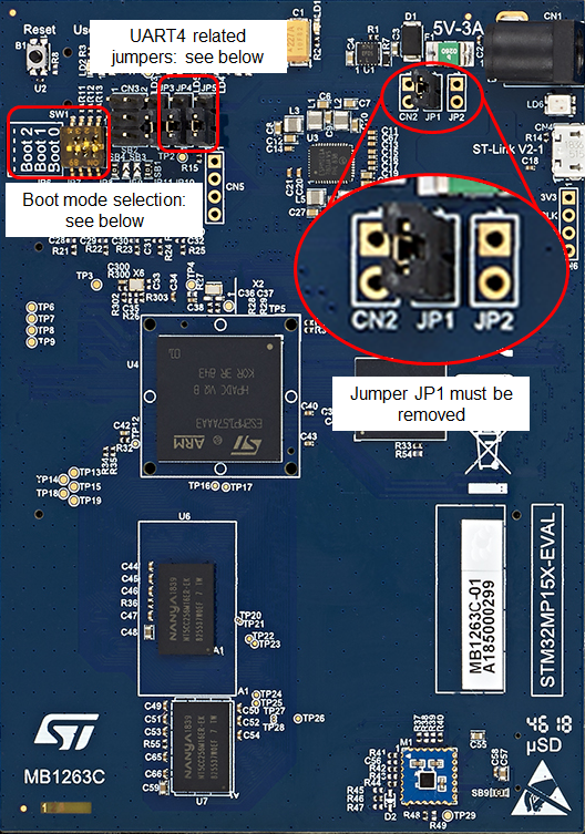
5. Switches and jumpers[edit | edit source]
Most of default settings of the switches and jumpers shall be kept as set in the commercial box.
There are 3 main exceptions:
- the jumpers related to UART4
- the switches related to boot
- the jumper JP1 that must be removed
The picture and sections below detail the main boot switches and the UART4 jumpers.
[edit | edit source]
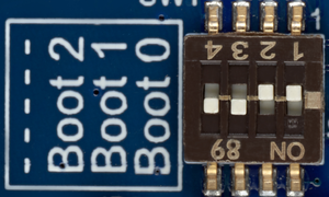
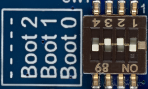
The STM32MP157x-EV1 Evaluation boards can boot from different Flash devices (microSD, eMMC...); using the microSD card is recommended.
| Boot mode | Boot 2 | Boot 1 | Boot 0 |
|---|---|---|---|
| Engineering boot | 1 | 0 | 0 |
| NOR | 0 | 0 | 1 |
| microSD card | 1 | 0 | 1 |
| eMMC | 0 | 1 | 0 |
| NAND | 0 | 1 | 1 |
| Forced USB boot for flashing |
0 | 0 | 0 |
The boot related switches (SW1 on the board overview picture) must be configured as illustrated by one of the following pictures:

[edit | edit source]
The UART4 is shared exclusively between 2 connectors:
- RS232, D-type, 9-pin connector (CN12 on the board overview picture), dedicated to communication through RS232,
- USB micro-B (ST-LINK/V2-1) (CN4 on the board overview picture), dedicated to the RS232 of ST-LINK/V2-1 controller
The connection is switched by setting JP4 and JP5 jumpers as shown in following pictures:
 UART4 is connected to the RS232, D-type, 9-pins CN12 connector |
 UART4 is connected to the USB micro-B ST-LINK/V2-1 CN4 connector |
6. GPIO mapping[edit | edit source]
6.1. Motor control connector[edit | edit source]
The pins of the motor control connector (CN22 on the board overview picture) are described in the following table.
Due to the sharing of some IOs by multiple peripherals, the motor control interface is not enabled by default, and the motor control cannot be operated simultaneously with the camera, audio codec, CAN and GPIO expansion (GPIO6, 7 and 12): more details (e.g. enabling the motor control interface) in the STM32MP157x-EV1 Evaluation boards user manuals.
| Description | Function | STM32 pin | Pin | Pin | STM32 pin | Function | Description |
|---|---|---|---|---|---|---|---|
| Emergency Stop | TIM8_BKIN | PA6 | 1 | 2 | - | - | GND |
| MC_UH | TIM8_CH1 | PI5 | 3 | 4 | - | - | GND |
| MC_UL | TIM8_CH1N | PH13 | 5 | 6 | - | - | GND |
| MC_VH | TIM8_CH2 | PI6 | 7 | 8 | - | - | GND |
| MC_VL | TIM8_CH2N | PH14 | 9 | 10 | - | - | GND |
| MC_WH | TIM8_CH3 | PI7 | 11 | 12 | - | - | GND |
| MC_WL | TIM8_CH3N | PH15 | 13 | 14 | PA3 | ADC_1_IN15 | Bus Voltage |
| PhaseA current | ADC_1_IN6 | PF12 | 15 | 16 | - | - | GND |
| PhaseB current | ADC_1_IN0 | ANA0 | 17 | 18 | - | - | GND |
| PhaseC current | ADC_2_IN1 | ANA1 | 19 | 20 | - | - | GND |
| NTC ByPass | GPIO | PF3 | 21 | 22 | - | - | GND |
| Dissipative Brake | TIM12_CH1 | PH6 | 23 | 24 | - | - | GND |
| 5V | - | - | 25 | 26 | PF11 | ADC_1_IN2 | Heatsink Temperature |
| PFC Sync | TIM4_ETR | PE0 | 27 | 28 | - | - | 3V3 |
| PFC PWM | TIM4_CH3 | PB8 | 29 | 30 | - | - | GND |
| Encoder A | TIM5_CH1 | PH10 | 31 | 32 | - | - | GND |
| Encoder B | TIM5_CH2 | PH11 | 33 | 34 | PH12 | TIM5_CH3 | Encoder Index |
6.2. GPIO expansion connector[edit | edit source]
The pins of the GPIO expansion connector (CN21 on the board overview picture) are described in the following table:
| Function | STM32 pin | Pin | Pin | STM32 pin | Function |
|---|---|---|---|---|---|
| 3V3 | - | 1 | 2 | - | 5V |
| GPIO2 / I2C5_SDA[EX 1] | PA12 | 3 | 4 | - | 5V |
| GPIO3 / I2C5_SCL[EX 1] | PA11 | 5 | 6 | - | GND |
| GPIO4 / MCO1 | PI11 | 7 | 8 | PB10 | GPIO14 / USART3_TX |
| GND | - | 9 | 10 | PB12 | GPIO15 / USART3_RX |
| GPIO17 / USART3_RTS | PG8 | 11 | 12 | PI5 | GPIO18 / SAI2_SCKA [EX 2] |
| GPIO27 / SDMMC3_D3 | PD7 | 13 | 14 | - | GND |
| GPIO22 / SDMMC3_CK | PG15 | 15 | 16 | PF1 | GPIO23 / SDMMC3_CMD |
| 3V3 | - | 17 | 18 | PF0 | GPIO24 / SDMMC3_D0 |
| GPIO10 / SPI1_MOSI | PZ2 | 19 | 20 | - | GND |
| GPIO9 / SPI1_MISO | PZ1 | 21 | 22 | PF4 | GPIO25 / SDMMC3_D1 |
| GPIO11 / SPI1_SCK | PZ0 | 23 | 24 | PZ3 | GPIO8 / SPI1_NSS |
| GND | - | 25 | 26 | - | GPIO7 / RPI_GPIO7 |
| ID_SD / I2C2_SDA | PH5 | 27 | 28 | PH4 | ID_SC / I2C2_SCL |
| GPIO5 / MCO2 | PG2 | 29 | 30 | - | GND |
| GPIO6 / TIM2_CH4 | PA3 | 31 | 32 | PH6 | GPIO12 / TIM12_CH1 |
| GPIO13 / TIM8_CH4 | PI2 | 33 | 34 | - | GND |
| GPIO19 / SAI2_FSA[EX 2] | PI7 | 35 | 36 | PI10 | GPIO16 / USART3_CTS |
| GPIO26 / SDMMC3_D2 | PF5 | 37 | 38 | PI6 | GPIO20 / SAI2_SDA[EX 2] |
| GND | - | 39 | 40 | PF11 | GPIO21 / SAI2_SDB[EX 2] |
- ↑ 1.0 1.1 The I2C5 is shared between the I2C EXT connector and the GPIO expansion connector. By default, the I2C5 is connected to the I2C EXT connector thanks to Solder Bridges: more details in the STM32MP157x-EV1 Evaluation boards user manuals.
- ↑ 2.0 2.1 2.2 2.3 The SAI2 is shared between the audio codec and the GPIO expansion connector. By default, the SAI2 is connected to the audio codec thanks to Solder Bridges: more details in the STM32MP157x-EV1 Evaluation boards user manuals.
6.3. JTAG connector[edit | edit source]
The pins of the JTAG connector (CN14 on the board overview picture) are described in the following table:
| Function | Pin | Pin | Function |
|---|---|---|---|
| Power | 1 | 2 | Power |
| NJTRST | 3 | 4 | GND |
| JTDI | 5 | 6 | GND |
| JTMS / SWDIO | 7 | 8 | GND |
| JTCK / SWCLK | 9 | 10 | GND |
| Pull down | 11 | 12 | GND |
| JTDO / SWO | 13 | 14 | GND |
| NRST | 15 | 16 | GND |
| Pull down | 17 | 18 | GND |
| pull down | 19 | 20 | GND |
6.4. User buttons and LEDs[edit | edit source]
The GPIO assignments for the user buttons and LEDs are described in the following table. Refer to LEDs and buttons on STM32 MPU boards article to get information on the functional mapping for each one.
| LED color and label | Button label | GPIO |
|---|---|---|
| Green LD3 (*) | USER1 (*) | PA14 |
| Red LD2 (*) | USER2 (*) | PA13 |
| Orange LD4 | - | PD8 |
| Blue LD5 | - | PD9 |
7. References[edit | edit source]