1. STM32WB dual core
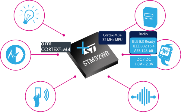
STM32WB combines an Arm® Cortex®-M4 processor for the application, plus a 2.4-GHz radio subsystem and an Arm® Cortex®-M0+ processor for running the firmware upgrade service (FUS) and the wireless stack.
| STM32WB dual core |
|---|
All code running on the Arm® Cortex®-M0+ processor (CPU2) is delivered as encrypted binary, and upgrading the wireless stack is necessary prior to any application project development.
All code running on the Arm® Cortex®-M4 processor (CPU1) is delivered as source code.
STM32WB is preloaded with root security system (FUS) firmware that is necessary for authenticating the selected wireless stack (binary encrypted format) loaded by the customer on st.com.
| STM32WB memory mapping |
|---|
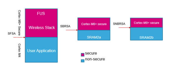
The Cortex®-M0+ security protects the upper parts of the flash and SRAM2 memories. The size of these areas is automatically set during the wireless stack installation or update:
- The secure flash memory start address (SFSA) is the lower boundary of the protected flash memory. It is aligned on a granularity of 4 Kbytes (for STM32WB5x) or 2 Kbytes (for STM32WB1x).
- For the STM32WB5x and STM32WB3x families:
- The secure backup RAM start address (SBRSA) and secure non-backup RAM start address (SNBRSA) are the lower addresses of the protected parts of the SRAM2a and SRAM2b memories respectively. The size can be set with a granularity of 1 Kbyte.
- Backup SRAM2a can be used to store data when the system is in standby mode.
2. System and memory overview
2.1. System architecture
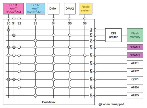
Here is a high-level overview of the system architecture:
- CPU: STM32WB features two Arm® Cortex®-M processors: a Cortex®-M4 and Cortex®-M0+ processor. The Cortex®-M4 processor is the main processor and runs at a maximum speed of 64 MHz, while Cortex®-M0+ is used for low-power tasks and runs at a maximum speed of 32 MHz.
- Memory: STM32WB has up to 1 Mbyte of flash memory and up to 256 Kbytes of SRAM. It also has a 32-Kbyte backup SRAM, which can be used to store data, even when the device is in low-power mode.
- Radio: The STM32WB radio subsystem supports Bluetooth® Low Energy 5.0 and IEEE 802.15.4 communication protocols.
- Peripherals: STM32WB has a wide range of peripherals, including timers, ADCs, DACs, SPI, I2C, UART, USB, and more. It also has a hardware encryption engine for secure data transmission.
The product datasheet is available here.
2.2. Memory system
The STM32WB memory organization was designed for flexibility, efficiency, and security.
2.2.1. Flash memory
- Up to 1 Mbyte of flash memory with a single-bank architecture:
- STM32WB55xG: 1 Mbyte of flash memory.
- STM32WB55xE: 512 Kbytes of flash memory.
- STM32WB55xC: 256 Kbytes of flash memory.
- STM32WB50xG: 1 Mbyte of flash memory.
- Accessible from address 0x0000 0000 or 0x0800 0000 (physical address).
- 4-Kbyte page granularity.
- Fast erase (22 ms).
- Fast programming time (82 μs for a double word).
The device flash memory is organized as follows:
- A main memory block containing 256 pages of 4 Kbytes. Each page contains eight rows of 512 bytes.
- An information block containing the STMicroelectronics bootloader (system memory), user data (OTP), and option bytes for user configuration.
| Flash area | Flash memory address | Size | Name |
|---|---|---|---|
| Main memory | 0x0800 0000 - 0x0800 0FFF | 4 Kbytes | Page 0 |
| … | … | … | |
| 0x080F F000 - 0x080F FFFF | 4 Kbytes | Page 255 | |
| Information block | 0x1FFF 0000 - 0x1FFF 6FFF | 28 Kbytes | System memory |
| 0x1FFF 7000 - 0x1FFF 73FF | 1 Kbytes | OTP area | |
| 0x1FFF 8000 - 0x1FFF 807F | 128 bytes | Option bytes |
2.2.2. SRAM memory
- Internal SRAM1:
- STM32WB55xG: 192 Kbytes SRAM1 @ 0x2000 0000
- STM32WB55xE: 192 Kbytes SRAM1 @ 0x2000 0000
- STM32WB55xC: 64 Kbytes SRAM1 @ 0x2000 0000
- STM32WB50xG: 64 Kbytes SRAM1 @ 0x2000 0000
- Internal SRAM2a (32 Kbytes) + SRAM2b (32 Kbytes) @ 0x2003 0000
3. Radio system
The radio system in STM32WB devices is a key feature of the microcontroller, as it enables wireless communication using Bluetooth® Low Energy and IEEE 802.15.4 protocols.
The radio system consists of a transceiver, a balun, and a power amplifier, and is designed to provide reliable and efficient wireless communication with low-power consumption.
The radio system in STM32WB devices includes a 2.4-GHz RF front end and a Bluetooth® Low Energy and IEEE 802.15.4 physical-layer controller. The radio system is controlled from the CPU2, which contains the radio lower-protocol software layers.
4. General-purpose I/Os (GPIOs)
The GPIO pins on STM32WB can be configured in a variety of modes, including input, output, alternate function, and analog. The pin mode can be configured using the device registers.
General information can be found on the GPIO wiki page.
5. Communication interfaces
5.1. USART/UART
The USARTs in STM32WB devices support synchronous and asynchronous communication modes, allowing them to communicate with a wide range of devices.
Main USART features:
- Full-duplex asynchronous communication.
- Two internal FIFOs for transmitting and receiving data.
- Synchronous controller/target mode and clock output/input for synchronous communications.
USART signals:
Bidirectional USART communications require a minimum of two pins: Receive Data In (RX) and Transmit Data Out (TX).
STM32WB devices have:
- 1x USART (ISO 7816, IrDA, SPI controller, Modbus, and smartcard mode).
- 1x LPUART (low-power).
General information can be found on the UART wiki page.
5.2. Other advanced communication interfaces
- 2x I2Cs (SMBus/PMBus).
- 2x SPIs up to 32 MHz.
- 1x serial audio interface (SAI) with two channels and three PDMs.
- 1x USB 2.0 FS device with embedded crystal-less oscillator, supporting BCD and LPM, and one quad-SPI with execute-in-place (XIP) capability.
6. IPCC
IPCC, which stands for inter-processor communication controller, is a communication interface available on STM32WB microcontrollers. IPCC is used to enable communications between the Cortex®-M4 and Cortex®-M0+ processors.
It provides six full-duplex channels:
- Six channels from processor 1 to processor 2.
- Six channels in the opposite direction.
In a Zigbee application, IPCC is used to enable communication between the Zigbee protocol stack running on the Cortex®-M0+ processor and the application running on the Cortex®-M4 processor.
7. Power supply management
STM32WB is designed for extremely low power consumption. The devices integrate an SMPS step-down converter to improve low-power performance when the VDD voltage is high enough. The SMPS converter can also be switched on or set to bypass mode at any time by the software application.
The device has different voltage supplies:
- VDD = 1.71 to 3.6 V: external power supply for I/Os and system functions, such as RF, SMPS, reset, power management, and internal clocks.
- VDDA = 1.62 (ADC/COMPs) to 3.6 V: independent power supplies for analog input for ADC and comparators.
- VDDUSB = 3.0 to 3.6 V: external, independent power supply for USB transceivers.
STM32WB devices support several low-power modes to achieve the best compromise between low-power consumption, short startup time, available peripherals, and available wake-up sources.
It is up to the user to select one of these low-power modes:
- Sleep.
- Low-power run.
- Low-power sleep.
- Stop 0, Stop 1, and Stop 2.
- Standby.
- Shutdown.
Refer to section 3.7.5 of the product datasheet for more details.
8. STM32WB development ecosystem
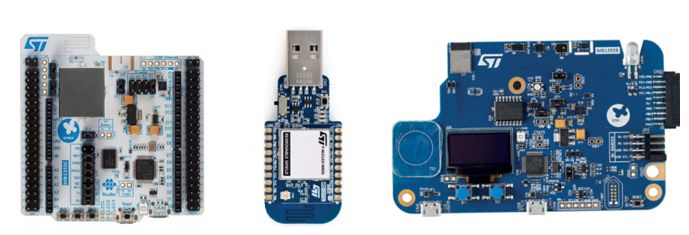
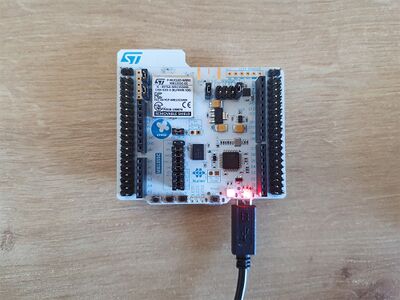
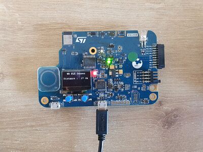
STM32WB can be used with a variety of development boards, including the STM32WB55 Nucleo pack, the STM32WB Nucleo boards, and the STM32WB discovery board.
| Development boards |
|---|
9. ST-LINK USB cable connections for P-NUCLEO-WB55 and STM32WB5MM-DK Discovery kit boards
The USB cable from the PC is used to power and interact with the STM32:
- P-NUCLEO-WB55: jumper JP1 to USB STL and USB ST-LINK to be used.
- STM32WB5MM-DK Discovery kit: jumper JP2 to 1-2 and USB ST-LINK to be used.
| Nucleo | Discovery kit |
|---|---|
10. Log via UART
STM32WB platforms embed the ST-LINK/V2 in-circuit debugger and programmer for STM32 microcontrollers. The single-wire interface module (SWIM) and JTAG/serial wire debugging (SWD) interfaces are used to communicate with the STM32WB microcontroller. It also supports the STM32 virtual COM port driver for communication between a PC and the application processor via a serial interface.
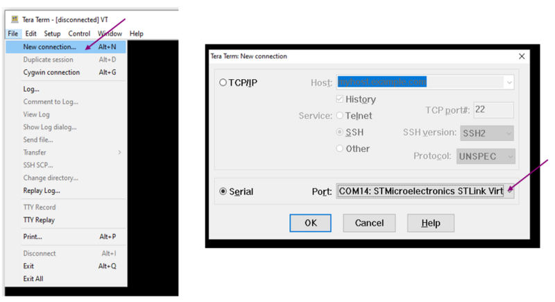
Use any convenient software terminal to open the serial communication port of the PC to check the messages from the board. Select your serial port and set up your connection as follows (the example below uses Tera Term software).
Set up a new serial connection to the STMicroelectronics platform:
| Tera Term setup (1/2) |
|---|
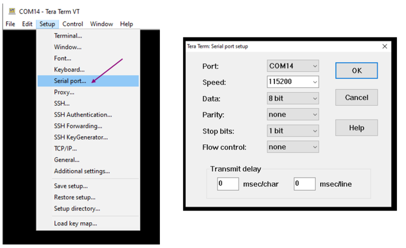
Set up your serial connection as shown below:
| Tera Term setup (2/2) |
|---|
