1. Introduction
This article covers general aspects about designing power supplies for STM32 based applications. It provides general guidelines on important characteristics, how to choose components, and optional features related to power supplies.
The first part is about power supplies in general.
- Define the main characteristics of power supplies and their impacts on applications.
- Talk about types switched-mode power supply (SMPS) and low dropout regulator (LDO) and compare them.
- Provide important power management considerations.
The second part specifies STM32 requirements regarding power supplies (PS).
- Power architecture of STM32.
- STM32 specific requirements regarding power supplies.
- How to identify the requirements of the application.
- Included features in STM32.
2. General notions power supply
Power supply quality is fundamental for the reliability of any electronic application. The purpose of this section is to get an overview of considerations about power supplies.
Ideally an electronic application must be supplied with a fixed voltage, response very fast to current calls and without any noise.
Applications are powered by an external source of electricity that can be a battery, a USB cable, or AC current for example. These sources can be noisy, especially if they supply power applications such as motors. Furthermore, the voltage can vary a lot, in the case of batteries depending on the charge and loading current.
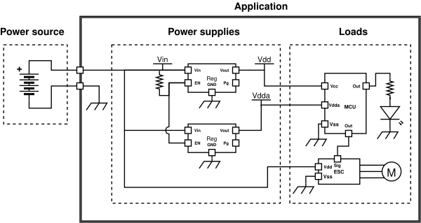
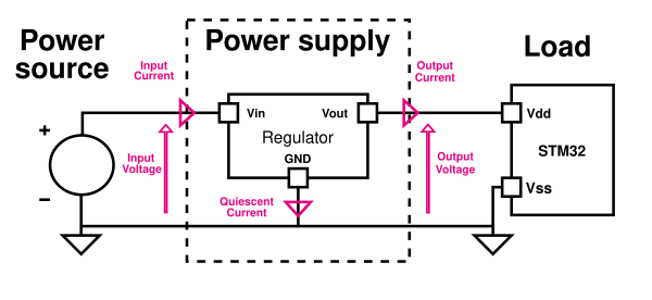
The role of the power supply is to generate a steady supply voltage for the application, independent from the input voltage and output current variations. In this document a difference is made between power source and power supply.
- Application: Scope of the engineering process.
- Power source: External energy source given with certain characteristics. Outside of the application.
- Power supply: System that converts voltage from the power source to the load that must match the power source and load characteristics. Inside the application.
- Load: Every component that consumes current from the power supply.
For more information about supplies topology for a wide variety of applications and components references see this guide: Power management guide
As current exists in two major forms, Alternative (AC) and Continuous (DC) power supplies are categorized by their type of conversion AC/DC, DC/DC, DC/AC (invertor) and AC/AC. In this topic we will only cover DC/DC supplies.
2.1. General definitions
2.1.1. Voltage
- Input Voltage
Power supplies are designed to handle a range of input voltages, see operating voltage in datasheet electrical characteristic table. If voltage spikes from the power source exceed this limit, it can lead to destruction of the power supply, and the whole application. The chosen component must handle the highest voltage spikes and not only the average voltage. Even short spikes can damage components.
- Output Voltage
The loads datasheet provides a range of operating voltages. The load might not work properly if applying insufficient voltage, on the other hand exceeding maximum value may lead to irreversible damage. The nominal output voltage must match the operating voltage of loads.
Transients are also to be considered. Dips are short drops of voltage. Swells are the inverse; it is a short overshoot of the voltage level. These phenomena can occur while load current transient phases or input voltage transient phases. Various aspects are covered in different sections of this wiki: Noise, Power management.
2.1.2. Current
- Max continuous current
The max continuous current corresponds to the consumption of the load in the worst-case scenario. The power supply must be able to provide this much current continuously. This gives the minimum requirement for the power supply max continuous current.
- Peak current
Peak currents are short time current spikes that occur in transient phases like power up, clock frequency shifting, high load I/O switching.
- Inrush current
In addition, the circuit contains capacitors. At power up these capacitors draws a huge amount of current to charge, this must be handled by the power supply.
- Average current
The average current is helpful to estimate energy consumption and size of finite or limited power source, like a battery, to ensure lifetime. It is also possible to have a power supply that only delivers the average current and use local electricity storage like capacitors to absorb transient currents.
- Quiescent current (IQ)
Quiescent current, IQ, is the consumption of the power supply itself. This may be negligible with medium or high currents but becomes significant in low power applications.
2.1.3. Noise
This section only talks about noise as choosing criteria for supply, refer to section Power management Decoupling to get more information about noise in general and good practice.
Some applications are especially sensitive to noise like precision analog devices or high frequency digital ICs.
There are different notions related to noise regarding power supply:
- Intrinsic noise
The physical properties of transistors and resistors imply noise. This source of noise is independent from the input, it is generated by the regulator itself, in particular the retroaction loop.
- Switching ripple (SMPS)
In SMPS Power supply SMPS, the voltage regulation is done by switching a transistor at high-speed rate (~50kHz-2MHz), this induces voltage variation on output. The amplitude of the ripple mainly depends on the size of the inductance, the output capacitor, and the output current. This constitutes the main disadvantage of SMPS.
- Power-Supply Rejection Ratio (PSRR)
PSRR is the ability of the power supply to reject input noise coming from the power source. It is like the power supply acts as a filter. The PSRR value is often given in datasheets. This is an important characteristic for low noise applications.
2.1.4. Efficiency
Power supply efficiency is an important factor in power consumption. In many cases energy is a limited or expensive resource. In ultra-low power applications, running on battery or induced current (RFID), efficiency is key to ensure high lifetime. In high power applications, power loss represents a significative amount of energy and a cost.
Furthermore, energy losses are dissipated in heat. If losses are concentrated in a small area, components may heat a lot and cause reliability issues.
Power supplies datasheets provide typical efficiency characteristics (In the case of LDO this is a bit different, look at the relative section).
2.2. Types of power supply
In DC/DC conversion, there are two major methods, linear regulator and SMPS (Switching Mode Power Supply).
2.2.1. Low Drop output (LDO)
Linear regulators are a low cost and easy way to regulate voltage. These are only step-down regulations with a minimal drop voltage, .
Low dropout regulators, LDO, are linear regulators with a low Vdrop, about 100 mV-500 mV, which allows output voltage very close to the input voltage.
The regulator itself does not introduce much noise relatively from SMPS. Thanks to that, LDOs are preferred for low noise application. These are characterized by their intrinsic noise and PSRR.
These types of power supplies are generally fully integrated and only require few simple components like resistor or capacitor.
To regulate the output voltage, LDO dissipates the difference in heat. . The major drawback is efficiency, (true for negligible quiescent current ), especially when the difference between Vin and Vout is huge. Because of that they are not recommended for 1 amp or higher current applications. Otherwise, make sure to have proper thermal dissipation.
Note: In low current application the quiescent current, IQ, of the LDO might become significative:
Note: Input current is equal to output current plus the quiescent current, current consumed by the LDO itself. The input current is not influenced by the voltage drop as LDO dissipates this drop in heat.
2.2.2. SMPS
Switching Mode Power Supplies are the most efficient way to regulate voltage, often between 80% and 90% up to 95% of efficiency for the best.
They are composed of switches, transistors, and diodes that chop the current and a strong L/C filter that convert chopped to continuous current and voltage.
There are different topologies of SMPS, the most common is the step-down Buck regulator.
The switching transistors generate ripples which are basically noise on Vout.
Note: PSRR is not relevant concerning SMPS
Note: There are low noise SMPS that are designed to have small ripples, but they have lower efficiency.
These types of power supplies are generally more expensive and take more place on the PCB. It requires higher value capacitors and an inductor.
SMPS are efficient in a certain range of power, so an over dimensioned SMPS is not only more expensive but also less efficient.
Note: Input current is equal to plus the current consumed by the SMPS itself. The input current is smaller when the voltage drop is higher as the SMPS converts power with minimal dissipation.
Note: As SMPS requires more decoupling capacitors, the inrush current is bigger.
2.2.3. Comparing SMPS/LDO
SMPS are more efficient than LDO, especially with the important input/output voltage difference.
LDO are low-cost and easy to implement, where SMPS requires a coil and more space on the PCB.
LDO generates less noise than SMPS.
High PSRR LDO can be used on the output of a SMPS to reduce switching noise while achieving good efficiency.
2.3. Power management
2.3.1. Decoupling
To provide a steady voltage without variations and noise, decoupling is a key element in power supply design. Supply voltage variations are introduced by load(current) variations and power conversion (LDO/SMPS…).
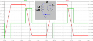
- Load current transient: Digital IC, motor control, communication IC, and most loads induce current variations. Any conductor has parasitic resistance and inductance that oppose to current variations. This results in voltage drop/peak across power lines. See illustrated below the voltage drop induces by current variation in an inductance:
- Not perfect power supply regulation: The active regulation as a latency to current variations. The retroactive loop introduces noise by measurement errors. In the case of SMPS there is also the ripple due to switching, see Noise section for more details.
- Power source: The third thing to consider is that the power source itself can be noisy for some reasons that are often imposed. Filtering can be required.
- Decoupling/Bypass capacitors
Decoupling consists of placing energy storage on different nodes of the power supply grid to locally supply these transient currents. These energy storages are capacitors placed as close as possible to transient generating circuits. The goal is to minimize the size of current loops to minimize parasitic resistors and inductance.
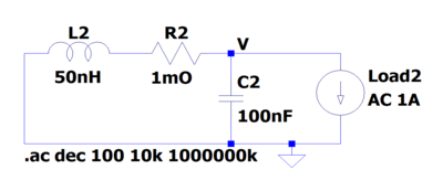
The figure above shows the frequency response with different decoupling capacitor. Serial coils amplify high frequencies, decoupling the capacitor cuts this amplification, the drawback is resonance frequency.
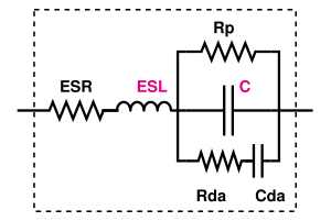
The second trouble is equivalent serial inductance (ESL). Components have parasitic inductances capacitance and resistance. The figure represents a common realistic capacitor model, in the case of decoupling we will focus on ESL.
Capacitor ESL depends mainly on technology and package type and size.
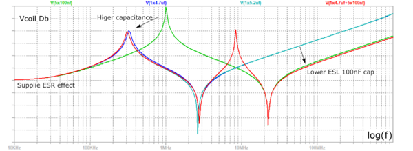
See in the figure below, that decoupling capacitors filter medium frequencies, but the ESL effect takes over at high frequencies.
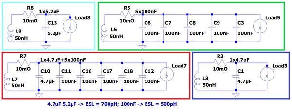
As bigger capacitors have higher ESL due to the bigger package, it is recommended to mix different sizes of capacitors to cover the widest band as shown in the figure below. Furthermore, placing multiple capacitors in parallel reduces equivalent serial inductance as .
For digital ICs like MCU, put a capacitor as close as possible to each VDD/Vss pin pair. If VDD pins are not close to Vss pins, put the capacitor close to VDD and directly to the ground plan.
It is important to select low ESR/ESL capacitors (equivalent serial resistance/inductance). Especially use ceramic SMD with the smallest package for a given capacitance. A bigger package has bigger ESL and ESR.
- Bulk capacitors
Bulk capacitors provide energy to the system to prevent voltage drops, they have generally large capacitance and are placed around the power supply.
In fact, the difference between decoupling, bypass, and bulk capacitor is not neat, all are used to stabilize voltage. Roughly bulk capacitors have bigger capacitance and provide more current for a longer period (filter lower frequencies).
In addition, for power supplies, these capacitors play two others major roles:
- Filter noise from the power supply itself, especially ripple from SMPS, and noise replicated from the power source.
- Power supply has feedback loops regulations that need capacitors to remain stable and accurate.
It is mandatory to respect the capacitors values given in datasheets.
In conclusion, capacitors play important roles in the supply path. It is important to pay attention to decoupling and PCB layout. Due to parasitic inductances in lines and capacitors and variety of frequencies to filter, one large capacitor is not equivalent to a properly sized one's placed at different places of the circuit.
Each component datasheet provides recommendations including application reference schematics.
2.3.2. Power on sequence
The power on sequence is the phase while the voltage is rising, and the components power on. The application is often composed of multiple ICs, which might have different startup voltage and delays. It is a good option to have a quick voltage rising ramp to prevent too much delay between two components startup. It is better to start from 0 V with all circuits fully discharged with no residual voltages, see Power down sequence for more information. The voltage curve must be monotonic and strictly rising.
The rising time is conditioned by the total capacitance (in Farads) of the circuit (chip + decoupling + components) as well as the impedance of the power supply ZSUPPLY or the current limit iMAX.
If the inrush current is too high, the voltage may drop during rising, and not be strictly rising or the power supply can shut off if an overcurrent protection is triggered. For more information, see section Current limiting.
2.3.3. Overcurrent protection
Most simple power supplies do not have any current management. In the case of short circuit or low impedance load, this can lead to destructive current for the power supply or the load. Furthermore, in some cases there are current limitations from the power source. To improve the quality and robustness of the application, it is recommended to choose a power supply with a current protection feature.
- Overcurrent cutoff
A simple solution is monitoring the current and cutting the power supply off when it reaches the limit. It is a simple and efficient solution, however if the threshold is too low, it can be triggered by a current spike like an inrush current.
- Current limiting
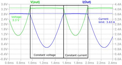
Power supplies with current limiting feature, adjust voltage to never exceed maximum current. This protects against short circuits and can be used to limit inrush current. It has the advantage of not power off completely in case of a transient spike of current. As illustrated in the figure below, the voltage drops when the current limit is reached, and the power supply switches in constant current mode.
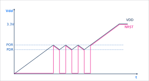
| Note: A current limiting can lead to a ripple around the startup voltage. When VDD passes over the power-on reset threshold, reset is released, and the STM32 starts to operate. If the current call is too high, the limiting current lowers the voltage, eventually enough to go back under the power-down reset threshold that resets the MCU. This can be repeated multiple times until the capacitors are eventually charged enough. The application resets multiple times before starting for good or may even never start. As illustrated in the side figure VDD oscillate around Nreset threshold. |
2.3.4. Soft start
Soft start is another way to control the inrush current. It consists of a controlled, slow voltage rising ramp.
Example components:
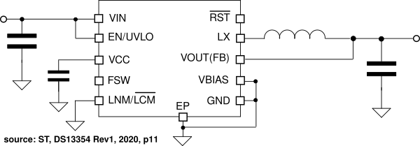
- L7983 is an SMPS controller that includes a soft start feature, the output voltage rises in 2 ms: DS13354 - Rev 1, ch 5.4, p17.
- LD59150 is an LDO with a programmable soft start and a power-good signal: DS12455 - Rev 7, ch 6.2, p8.
2.3.5. Over voltage protection (OVLO)
Overvoltage lockout (OVLO) feature cuts output power when the voltage reaches an overvoltage threshold. This prevents damaging the load in case of unexpectedly high input voltage. STBP120 is a power supervisor IC that provides multiple features including OVLO.
2.3.6. Under voltage lockout (UVLO)
Under voltage lockout consist of cutting output power when the input voltage passes below a threshold. This prevents powering the load with an intermediate voltage. The ST1PS03 is a buck converter (SMPS) which includes under voltage lockout.
2.3.7. Power-good signal
Power-good signal can be provided either by the power supply itself or by a power monitor device, tells when the voltage is high enough and stabilized. Is useful to keep reset an IC during supply startup to play the role of internal Power supply supervisor. It is also used to enable another power supply to manage power one order for example.
For example, LDL40 and LD59150 are LDO with an integrated PG feature.
Here finds an external power supervisor that implements some functionalities presented above: https://www.st.com/en/reset-and-supervisor-ics.html.
2.3.8. Power down sequence
The importance of power down phase is frequently underestimated. It is recommended to always keep a low impedance tied on VDD, even for the power down phase. To properly discharge all capacitance, pull VDD below tens of millivolts with a low impedance. There are different methods to implement proper power down.
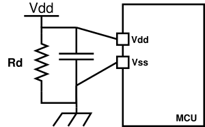
- Passive resistor
A resistor, RD, places between VDD and GND discharge capacitors when the power supply is off. Discharge time lasts about and C is the sum of all decoupling/bulk capacitors. This is a low-cost solution, but it consumes power permanently: . The lower the pull-down resistor, the quicker the discharge and higher is the consumption.
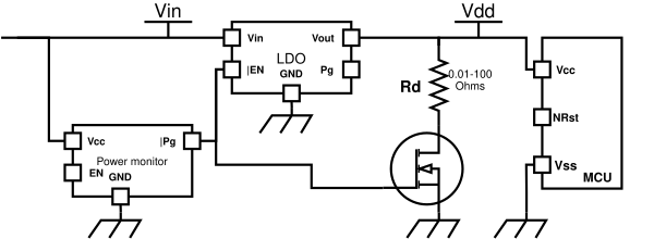
- Power monitor + Mos
This solution uses a resistor in series with a transistor controlled by an inverted power-good or enable signal. Two important elements to take care:
- Ensure that VDD rail is not powered when closing the discharge switch, either by disabling the regulator or be sure that no more power source is connected. Otherwise, this led to a huge current call.
- The discharge switch gate needs to be held above the VGS threshold until VDD rail reaches 0V. This can be challenging if Vin drops quickly. Consider these parameters to ensure a functional circuit:
- Use a low VGS N-Channel MOSFET transistor.
- Adding a capacitor in the power monitor supply domain can help to keep it powered longer.
- Use a lower resistor to discharge VDD rail quicker.
- Set a high Vin threshold to give more time margin.
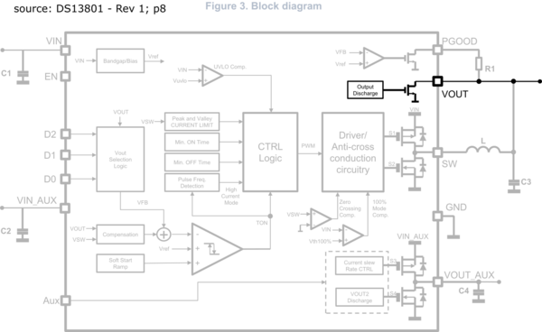
- PS integrated discharge
The most efficient way to implement this feature is to use a fully integrated in the power supply itself. This reduces overall complexity, conception time, number of components and used space on the PCB.
Some power supplies, equipped with an enable feature, has an internal switch that ties the Vout line to the ground when disabled.
For example, the STLQ020 is an LDO with an optional discharge feature through a 100 Ω resistor when the enable signal is low.
The ST1PS03 is a buck converter (SMPS) which includes an output discharge feature.
2.3.9. Components example
- ST1PS02 SMPS regulator; 400-mA buck regulator:
- Adjustable output current limit
- Power-good signal
- Constant current soft start
- Output discharge
- Under voltage protection
- ST1L08 LDO regulator; 800-mA high PSRR linear regulator:
- Power-good signal
- Current limiter
- Enable signal
- Thermal protection
- STEF05 eFuse:
- Soft start
- Output voltage clamp
- Current limiting
3. STM32
3.1. Context
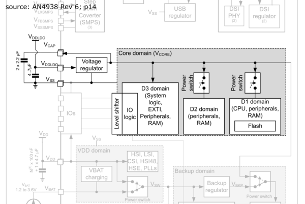
STM32 microcontrollers are composed of different power domains. This has different purposes:
- To have different operating voltage.
- To have different power sources.
- To shut down some parts to reduce power consumption.
- To isolate from perturbations.
The main supply of STM32 is called VDD. On the simplest products and/or the smallest packages, this is used to supply the entire device. Slightly more advanced products have other input power supplies dedicated to specific features like analog peripherals, GPIO, USB, SPI, LCD.
Some STM32 are internally divided into different power domains. They can be separated by power switches or regulators. Thanks to that some power domains can be completely unpowered when not used. For example, STM32H747/757 as explained in the [AN5215].
3.2. Specific supplies configurations
3.2.1. VCORE/VCAP
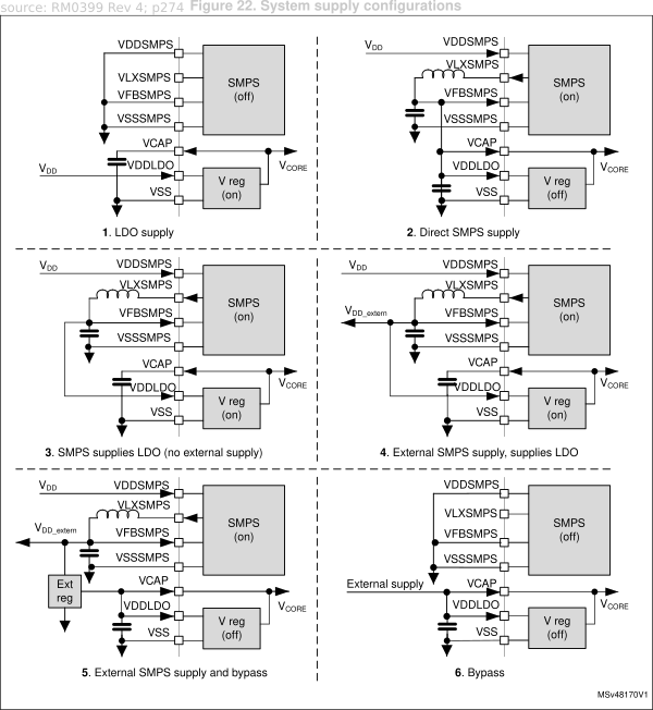
CPU, memory, and most of the digital peripherals are part of the Core domain or VCORE domain. This voltage rail is generally provided by an internal LDO. On some products, CPU voltage supply (VCORE) is externally accessible through VCAP pin, in this case there is different way to supply VCORE power domain:
- Internal LDO
LDO Supply (1st configuration) VCORE provided by the internal LDO supplied with VDD. This requires a decoupling capacitor on VCAP for the stability of the internal LDO.
- External regulator
Bypass (6th configuration) It is possible to externally supply VCORE through VCAP bypassing the internal LDO.
- Internal SMPS
In some devices, an internal SMPS is available. It can be used to be more efficient.
Direct SMPS supply (2nd configuration) The internal SMPS can supply directly VCORE to get better efficiency.
SMPS supplies LDO (3rd configuration) To reduce the ripple from SMPS, supply the internal LDO by the SMPS. The SMPS output is about 100 mV above VCORE, and the LDO filters the ripple.
Note: Depending on the configuration recommended, decoupling caps have different values.
Note: Some STM32 with VCAP available does not allow bypass of internal regulator. Always verify in the product datasheet or reference manual that supply configuration is allowed.
3.2.2. VDDA VREF
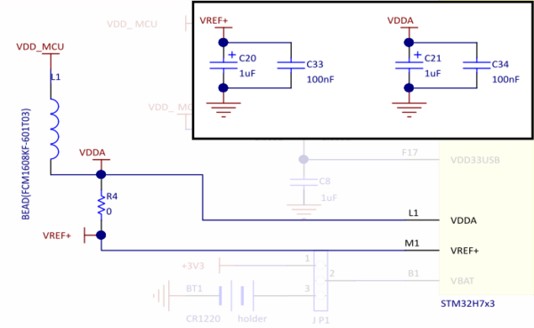
When VDDA pins are available on the packager, the analog power domain is separated from the digital power domain to reduce the impact of digital switching noise. Analog components such as ADC, comparators, DAC are supplied by VDDA.
For sensitive applications, VDDA can be provided by a separate power supply like a low noise and high PSRR LDO. If not possible, the minimal recommendation is to connect VDDA to VDD with a ferrite bead in series.
The main sensitive point regarding noise and accuracy is VREF, which is the voltage reference used by analog components. This means that ADC measurement accuracy and noise (SNR) directly dependent on VREF. VREF is generally accessible through VREF+ pin.
VREF can be provided in different ways.
- The simplest solution is to use VDDA. The smallest packages have VREF+ directly bounded to VDDA. Otherwise, it is possible to directly tie VREF+ and VDDA together. In this case, VDDA is more sensitive to noise and accuracy.
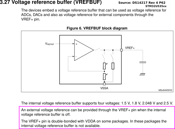
- Some products embed an internal bandgap reference VREFBUF which can provide a steady voltage reference that does not depend on VDDA precision and filter its noise. This adds a filtering step and is easy to implement as it is integrated inside the STM32. As trade of the bandgap reference consumes current. This configuration requires a capacitor in VREF+ pin.
- Finally, it is possible to provide an external reference through VREF+ pin provided by a dedicated component.
Decoupling: STM32 datasheets provide a decoupling scheme depending on the wiring of VREF.
In conclusion, noise and accuracy of analog devices depends on VREF noise and accuracy. Not respecting wiring and decoupling recommendation can lead to perturbations on VREF so impact analog devices performances.
3.3. Power consumption factors
There are multiple factors that influence the STM32 consumption.
3.3.1. Voltage
Digital IC consumes more current when operating at higher voltage. Some STM32 have a range of operating voltages, this able to choose the voltage level to reduce consumption. The core voltage VCORE selected by VOSx and peripherals such as VDDIO or VDDX voltage can be modulated depending on the product. Keep in mind that lowering the voltage lowers the maximum operating frequency. Important note: A current spike is drawn when increasing the voltage, a current spike that must be handled by the power supply.
3.3.2. Frequency
STM32 consumption depends on the clock frequency, the higher the clock speed is, the higher the current. Lowering the CPU or peripheral clock frequency helps to reduce the current consumption.
Important note: A current spike is drawn when increasing the frequency, a current spike that must be handled by the power supply.
3.3.3. Peripherals
On STM32 peripherals are dynamically configurable, they can be deactivated when not used. Deactivating a peripheral, by removing its clock, disconnecting IOs pins and reconfiguring registers, reduces overall consumption.
3.3.4. CPU Modes / Low power Modes
STM32 has different operating modes (Run, Sleep, Stop, Standby, Low power Run, Low power Sleep, ...) that enable/disable peripherals, functionalities, and change operating frequencies and voltage. These are used to reduce power consumption when some features are not used by the application.
See this article for more information: https://wiki.st.com/stm32mcu/wiki/Getting_started_with_PWR.
Note: Keep in mind that waking up MCU from sleep or stop modes take time and consume current. It is longer to wake up from deeper sleeping mode. Some parameters like clock frequency help to have a quicker wake up at the price of a higher peak current.
3.3.5. Temperature
The physical properties of materials, especially resistivity, are affected by temperature. Digital IC consumes significantly more at high temperatures.
3.3.6. Conclusion
Reducing voltage, frequency and deactivating unused peripherals reduces overall consumption. Keep in mind that increasing voltage, frequency, or reactivating voltage regulators or peripherals often induces a current spike.
3.4. How to estimate consumption
3.4.1. STM32CubeMX Power Consumption Calculator (PCC)
To estimate power consumption, STM32CubeMX software integrates a tool called Power Consumption Calculator (PCC). This is an interesting complementary tool to the manual approach presented in this chapter. See STM32CubeMX User manual (UM1718) chapter 13 "Using the Power Consumption Calculator to optimize the embedded application consumption and more" to learn more.
3.4.2. Configuration consumption
Many parameters can be configured dynamically during application execution, this modifies consumption. The first step is estimating consumption of different configurations.
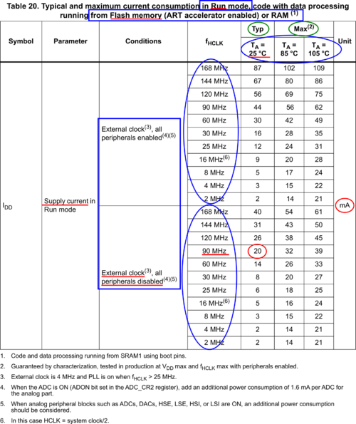
The first thing to look at is the system consumption. Datasheet usually system consumption with all peripherals disabled for different mode, clock, and memory configuration. The consumption includes Clock source, program memory and CPU. Note that datasheets usually give typical and maximum values at different temperatures.
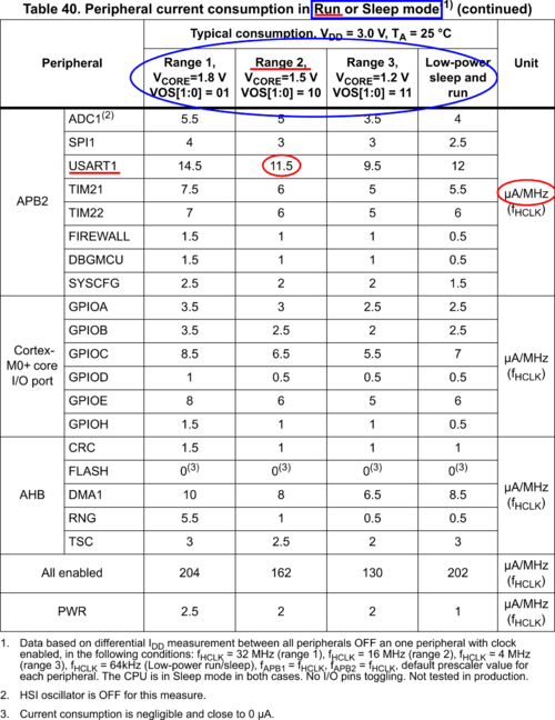
Then look at each peripheral consumption depending on their configurations.
The total consumption is the sum of all component's consumption. As generally CPU value is given for the whole MCU except peripherals, add to this each activated peripherals consumption.
Note: Current is measured at Vdd level, as shown in the current consumption measurement table in STM32 datasheets. For STM32 with integrated SMPS, datasheets provide different consumption values with internal LDO and internal SMPS.
Note: Current measurements are provided for the specific conditions specified in the datasheet.
| Example: STM32F405RG in run mode, executing code from flash memory, running at 90 MHz with all peripherals disabled consume 20 mA in typical conditions at 25°C: | Example: STM32L073V8 in run mode, Range 2 (VCORE = 1,5 V), FHCL = 16 MHz, FAPB2 = 8 MHz, the USART1 consume 11.5 µA/MHz so: 92 µA in typical conditions: |
3.4.3. Average current
To calculate the average current, sum the consumption of the CPU for each configuration pondered with time ratio spend in it, add to that the consumption of each peripheral at a given configuration pondered with use time ratio. The average current gives a long theme consumption, it is relevant to estimate the energy consumption and size of a finite energy source like a battery.
3.4.4. Maximum continuous current
Take the configuration that consumes the most in application conditions. This value must be lower than the maximum continuous current characteristic of the power supply.
3.4.5. Peak current
- Inrush
One of the main sources of peak current is the inrush during power-up. Supply voltage rise charge capacitors of the circuit and startup of ICs draw current. This represents a significative amount of energy.
The inrush current might be much higher than other currents spikes in operating conditions. To reduce the size of the power supply, it is possible to control inrush, either using a current limiting feature in the power supply or soft start, see Soft start section for more information.
Three elements are related, total capacitance, rising time and peak current. Always remember that tuning one affects the others.
Note: This topic is related to rising time, see Power on sequence section. The faster the voltage rises, the higher the current is. ; is the rising rate, CEQ equivalent capacitance of the system, sum of all decoupling/bulk capacitor, capacitance of the different components/chip.
- Mode transition
Transitioning between different run/operating modes, low power modes, clock frequency, voltage ranges induce transient current that might be significative for sensitive applications.
Wake-up consumption is given in the datasheet in Ampere seconds (Coulombs), it corresponds to the total charge consumed to wake up, here is the example of STM32U535:
| Wake up from | Stop1 | Stop3 | Standby | ||
|---|---|---|---|---|---|
| nAs (nano Coulombs) | 70 | 610 | 3200 | ||
| STM32U353 wakeup consumption from different modes | |||||
3.5. STM32 supply pins reference decoupling scheme
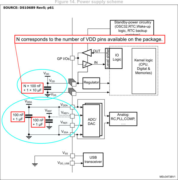
It is recommended to put small capacitors for each power supply pin, and some bigger for the whole circuit. In any case refer to the "Power supply scheme" figure in the device datasheet. When there is multiple power domain, decoupling is needed for each one. When VCAP is available, decoupling capacitors need to be attached as close as possible to VCAP pins.
Here is the example of the STM32L0: 100 nF for each supply pins and an additional 10 µF for each power domain.
- PCB recommendations
The PCB layout plays an important role in the quality of decoupling, refer to the Getting started application note, dedicated to the STM32 model, to get precise guidelines.
Generally speaking, it is important to have low-impedance power plans.
3.6. Power supply supervisor
To ensure that the MCU does not run under the minimum operating voltage, STM32 devices have integrated voltage monitoring circuitry.
3.6.1. System reset
A system reset sets all the registers to their default values except the reset flags in the clock controller RCCRSR register and the registers in the backup domain. A system reset is generated when one of the following events occurs:
- A low level on the NRST pin (external reset)
- Window watchdog end of count condition (WWDG reset)
- Independent watchdog end of count condition (IWDG reset)
- A software reset (Software reset)
- A low-power management reset.
3.6.2. Power-on reset (POR)/power-down reset (PDR)
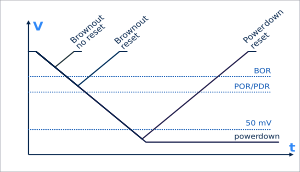
The STM32 remains in reset mode while VDD is below a specified threshold, VPOR/PDR, generally around 1.7V-1.8V. For more details concerning tRSTTEMPO and VPOR/VPDR threshold value, refer to the "electrical characteristics" and "reset and power control block characteristics table" in the MCU datasheet.
On some devices, the PDRON pin is available. In this case the power supply supervisor is enabled by holding PDRON high and can be disabled by pulling down PDRON. Otherwise, if not available the power supply supervisor is always enabled.
If a power supply supervisor is disabled, an external power supply supervisor must monitor VDD and control the NRST pin. The device must be maintained in reset mode as long as VDD is below the minimum operating voltage specified in the datasheet.
The supply ranges that never go below VPOR/PDR are managed more effectively using the internal circuitry (no additional components are needed, thanks to the fully embedded reset controller). When the embedded power supply supervisor is off, the following integrated features are no longer supported:
- The integrated power-on reset (POR) / power-down reset (PDR) circuitry is disabled.
- The brownout reset (BOR) circuitry must be disabled.
- The embedded programmable voltage detector (PVD) is disabled.
- The VBAT functionality is no longer available and the VBAT pin must be connected to VDD.
3.6.3. Brownout reset (BOR)
The BOR keeps the system under reset until the VDD supply voltage reaches the selected VBOR threshold.
BOR is enabled through the option bytes, as well as the VBOR threshold. Different BOR levels are available depending on the device. It is used to set a higher threshold than VPOR and can be modified dynamically, see the device reference manual or datasheet for more information.
3.6.4. Programmable voltage detector (PVD)
The PVD is an additional voltage monitoring system. It sets a flag that tells if VDD is above or below the selected threshold. PVD is activated and the threshold VPVD selected through registers, see the device reference manual or datasheet for more information.
It can be connected to the EXTI to trigger interruption when VDD drops below the selected threshold or rise above the threshold. As an example, the service routine can perform emergency shutdown tasks such as saving data in the backup domain.
The analog voltage detector (AVD) can be used to monitor the VDDA power supply like the PVD.
3.7. Multiple power supplies rules
3.7.1. Voltage differences
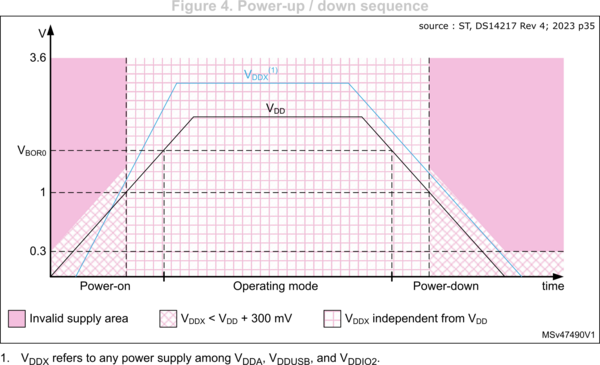
Different power domains have constraints about voltage differences. The datasheet specifies when one voltage needs to be higher than a second one, or the voltage difference might not exceed a certain value. For example, VDDA vs VDDX for STM32L0:
Here is the case of the STM32U5 product: VDDA VDDUSB and VDDIO2 vs VDD:
3.7.2. Circuit examples
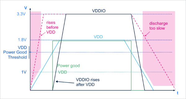
A simple way to ensure that a supply voltage VDDX does not rise before VDD, is to wire power-good signal from VDD regulator to enable the signal of VDDX regulator as shown in the figure below.
Also be sure that VDDX regulators have proper discharge feature to prevent any VDDX staying above VDD during the power down phase.
In the figure below, an example of the system above applied on VDDIO. In this example VDD is 1.8 V and VDDIO 3.3 V. VDDIO must not exceed VDD during rise and falling time. Note, during power down phase VDDIO must discharge fast enough to reach 1 V before VDD.
4. Glossary
4.1. General
- AC: Alternative Current
- ADC: Analog to Digital Convertor
- CPU: Central Processing Unit
- DAC: Digital to Analog Convertor
- DC: Direct Current
- ESL: Equivalent Serial Inductance
- ESR: Equivalent Serial Resistor
- GPIO: General Purpose Inputs Outputs
- IC: Integrated Circuit, general term for silicon chips.
- LDO: Low DropOut linear regulator
- MCU: MicroController Unit
- OVLO: Over Voltage Lock Out
- PCB: Printed Circuit Board
- PS: Power Supply
- PSRR: Power-Supply Rejection Ratio
- RFID: Radio Frequency IDentification
- SMPS: Switching Mode Power Supplies
- SNR: Signal to Noise Ratio, This corresponds to the noise level compared with signal level. This is commonly used to characterize signal treatments.
- SPI: Serial Peripheral Interface, serial communications interface
- STM32: STMicroelectronics microcontrollers 32 bits family
- USB: Universal Serial Bus, serial communications interface
- UVLO: Under voltage lockout
4.2. STM32 specific
- AVD: Analog Voltage Detector
- BOR: BrownOut Reset
- EXTI: EXTernal Interrupt,
- NRST: Not Reset signal, reset IC if low
- PDR: Power Down Reset
- PG: Power Good signal
- POR: Power On Reset
- PVD: Programmable Voltage Detector
- VCORE: supply voltage for digital core
- VDD: main supply voltage of circuit
- VDDA: supply voltage for analog peripherals
- VDDIO: supply voltage for GPIO
- VDDX: supply voltage for peripheral X
