 This article provides an overview of STM32MP257x-DK Discovery kits.
1. Article purpose[edit | edit source]
This article briefly describes:
- How to assemble together the different elements provided in the commercial box and additional optional accessories
- What are the different components present on the boards
- How to connect the boards to external material
- How to configure the board for boot
- What are the configurations of the connectors pins
This article is valid for the STM32MP257F-DK ![]() Discovery kit: the part numbers are specified in the STM32MP25 microprocessor part numbers article.
Discovery kit: the part numbers are specified in the STM32MP25 microprocessor part numbers article.
| This article is only an introduction to the STM32MP257x-DK Discovery kit. Detailed information can be found in the STM32MP257x-DK Discovery kits user manuals. |
2. Board assembly[edit | edit source]
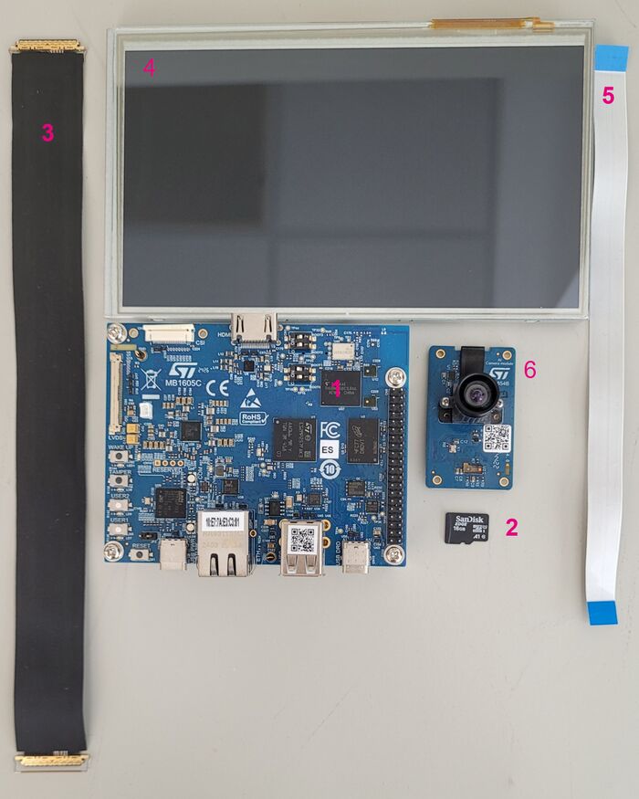
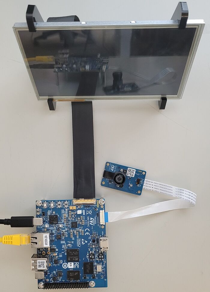
The STM32MP257x-DKx Discovery kits package (STM32MP257F-DK ![]() ) contains the items listed below.
) contains the items listed below.
| Position | Description |
|---|---|
| 1 | MB1605 motherboard |
| 2 | microSD card |

| To complete the basic setup, you can buy an LVDS display and a CSI camera |
The complete set will be then:
| Position | Description |
|---|---|
| 1 | MB1605 main board |
| 2 | MicroSD card |
| 3 | LVDS display cable (provided via B-LVDS7-WSVGA package) - optional |
| 4 | 7” LVDS WSVGA display with touch panel EDT ETML0700Z9NDHA panel provided via B-LVDS7-WSVGA package - optional |
| 5 | camera board FFC (provided via B-CAMS-IMX package) - optional |
| 6 | MB1854 board AI camera provided via B-CAMS-IMX package - optional |

2.1. How to connect LVDS display to ST board - optional[edit | edit source]

- Check the above cable orientation thanks to the black mark and the white twisted pairs.
- Find the LVDS port on STM32MP257x-DK Discovery kit (CN2) and the one on the display (CN1). One cable is provided in the LVDS display box.
- On each port, insert the cable as described:

2.2. How to connect MB1854 camera board to ST board - optional[edit | edit source]
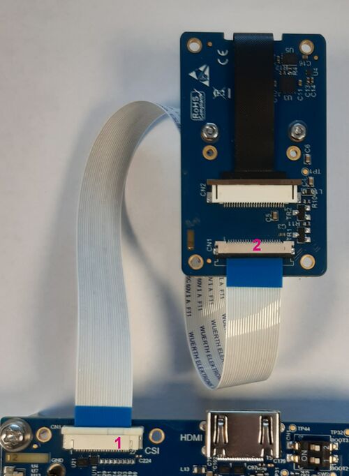
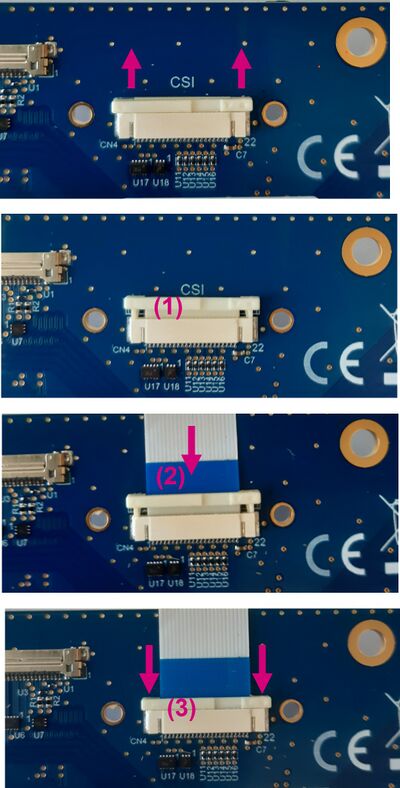
- Find the camera port on STM32MP257x-DK Discovery kit (CN8) (1 - in picture above) and the one on MB1854 (CN1) (2 - in picture above). One FFC is provided in the camera box.
- On each port, carefully:
- lightly pull the black plastic (1 - in picture below) to insert the contact side of the FFC towards the board (2 - in picture below).
- Push the black plastic to hold the FFC (3 - in picture below).
2.3. STM32MP257x-DK Discovery kit assembled[edit | edit source]
3. Board overview[edit | edit source]
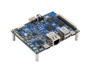
Main board MB1605, revision C-01: part of the STM32MP257x-DK Discovery kit ![]() .
.

Details about some LEDs:
- The LD11: turns green if power connection established (the power cable is inserted into the CN21 connector).
- Two general-purpose color LEDs (LED1 and LD9) are available as light indicators:
- The blue LED (LED1) is used as the Linux® Heartbeat LED, which is blinking as long as Linux® is alive on the Cortex®-A.
- The orange LED (LD9) is used as a STM32Cube example verdict LED.
- The two LEDs, the LD7 (red) and LD8 (green) are either connected to the STM32MP257 MPU ??? sentence coming form UM, not enough clear
- The LEDs (LD5 and LD6) are used as ST-LINK indicator status.
4. Board connection[edit | edit source]
The connections shown in the picture below are the ones recommended to start with the STM32MP257x-DK Discovery kits. As shown in the board overview, other connectors are available for this board (for example GPIO expansion connector).
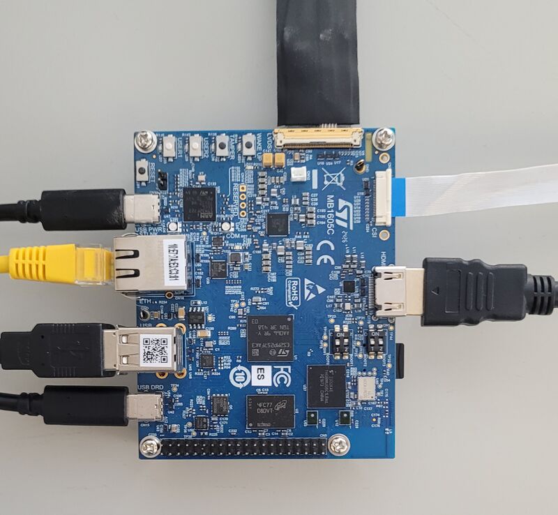
- MB1605 motherboard: STM32MP257F 14x14
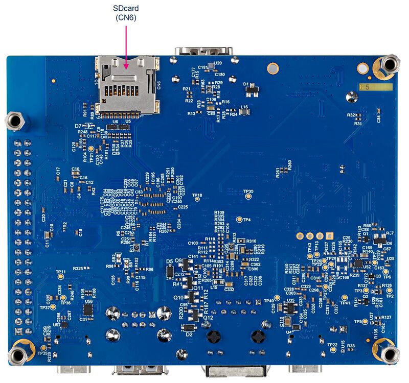
- MicroSD card slot, on back side
- 2 x USB type A (host) → E.g. mouse Keyboard USB driver...
- USB2.0 DRD TypeC → flashing via STM32CubeProgrammer
- Reset button
- Ethernet → Network
- USB Power Delivery TypeC → Power or STLINK
- HDMI→ TV Screen
- CSI camera connector
- LVDS display connector
5. Boot switches[edit | edit source]
The STM32MP257x-DK Discovery kit can boot from different Flash devices (microSD, eMMC); using the microSD card is recommended.
| Boot 3 | Boot 2 | Boot 1 | Boot 0 | Boot mode Cortex-A35 |
|---|---|---|---|---|
| 0 | 0 | 0 | 0 | Forced USB boot for flash programming |
| 0 | 0 | 0 | 1 | microSD card on SDMMC1 |
| 0 | 0 | 1 | 0 | eMMC on SDMMC2 |
| 0 | 0 | 1 | 1 | Development boot |
'1' is considered when switch is pushed in "ON" position and is ‘0’ otherwise.
The boot related switches (SW1 and SW2 on the board overview picture) must be configured as illustrated by one of the following pictures:


6. GPIO mapping[edit | edit source]
6.1. GPIO expansion connector[edit | edit source]
The pins of the GPIO expansion connector (CN5 on the board overview picture) are described in the following table:
| Function | STM32 pin | Pin | Pin | STM32 pin | Function |
|---|---|---|---|---|---|
| 3V3 | - | 1 | 2 | - | 5V |
| GPIO2 / I2C8_SDA | PZ3 | 3 | 4 | - | 5V |
| GPIO3 / I2C8_SDL | PZ4 | 5 | 6 | - | GND |
| GPIO4 / MCO1 | PF11 | 7 | 8 | PF13 | GPIO14 / USART6_TX |
| GND | - | 9 | 10 | PF14 | GPIO15 / USART6_RX |
| GPIO17 / USART6_RTS | PG5 | 11 | 12 | PD2 | GPIO18 / SAI2_SCKA |
| GPIO27 | PZ9 | 13 | 14 | - | GND |
| GPIO22 | PZ0 | 15 | 16 | PZ1 | GPIO23 |
| 3V3 | - | 17 | 18 | PZ6 | GPIO24 |
| GPIO10 / SPI6_MOSI | PC7 | 19 | 20 | - | GND |
| GPIO9 / SPI6_MISO | PC4 | 21 | 22 | PZ7 | GPIO25 |
| GPIO11 / SPI6_SCK | PF7 | 23 | 24 | PF4 | GPIO8 / SPI6_NSS |
| GND | - | 25 | 26 | PZ5 | GPIO7 |
| I2C2_SDA | PF0 | 27 | 28 | PF2 | I2C2_SCL |
| GPIO5 / TIM8_CH4 | PC10 | 29 | 30 | - | GND |
| GPIO6 / TIM5_CH1 | PH8 | 31 | 32 | PA5 | GPIO12 / TIM2_CH4 |
| GPIO13 / TIM4_CH2 | PA1 | 33 | 34 | - | GND |
| GPIO19 / SAI4_FSA | PD0 | 35 | 36 | PF15 | GPIO16 / USART6_CTS |
| GPIO26 | PZ8 | 37 | 38 | PD1 | GPIO20 / SAI4_SDA |
| GND | - | 39 | 40 | PB5 | GPIO21 / SAI4_SDB |
6.2. User buttons and LEDs[edit | edit source]
The GPIO assignments for the user buttons and LEDs are described in the following tables. Refer to LEDs and buttons on STM32 MPU boards article to get information on the functional mapping for each one.
| LED color and label | GPIO |
|---|---|
| Green LD8 | PH5 |
| Red LD7 | PH4 |
| Orange LD9 | PH6 |
| Blue LED1 | PH7 |
| Button | GPIO |
|---|---|
| USER1 | PC5 |
| USER2 | PC11 |
7. References[edit | edit source]