Registered User mNo edit summary |
Registered User m (Ensure uniformity of punctuation across the document in bullet list. Correct the phrase "allows to demonstrate" to a more appropriate form. Correct the phrase "associate software" to "associated software." Add Oxford commas where necessary. Correct the badly formed sentence "can be used assigned to the different execution contexts." Correct any verb tense errors.) Tag: 2017 source edit |
||
| (4 intermediate revisions by 2 users not shown) | |||
| Line 9: | Line 9: | ||
This article shows the default memory mapping defined by STMicroelectronics in [[STM32MPU Embedded Software architecture overview|STM32MPU Embedded Software]]. It uses a subset of all memory regions that are exposed at hardware level: customers may use other memory regions or aliases that are not shown here but are described in the [[STM32MP25 resources#Reference manuals|STM32MP25 reference manuals]].<br /> | This article shows the default memory mapping defined by STMicroelectronics in [[STM32MPU Embedded Software architecture overview|STM32MPU Embedded Software]]. It uses a subset of all memory regions that are exposed at hardware level: customers may use other memory regions or aliases that are not shown here but are described in the [[STM32MP25 resources#Reference manuals|STM32MP25 reference manuals]].<br /> | ||
The objective of the default [[STM32MPU Embedded Software architecture overview|STM32MPU Embedded Software]] memory mapping is to propose a generic memory mapping that: | The objective of the default [[STM32MPU Embedded Software architecture overview|STM32MPU Embedded Software]] memory mapping is to propose a generic memory mapping that: | ||
* allows | * allows demonstrating all the features proposed by the hardware platform and associated software. | ||
* is compliant with the official ST boards | * is compliant with the official ST boards. | ||
== Memory mapping == | == Memory mapping == | ||
| Line 25: | Line 25: | ||
rect 120 340 698 396 [[STM32MP2 SRAM internal memory | SRAM]] | rect 120 340 698 396 [[STM32MP2 SRAM internal memory | SRAM]] | ||
rect 120 311 698 340 [[RETRAM internal memory| RETRAM]] | rect 120 311 698 340 [[RETRAM internal memory| RETRAM]] | ||
rect 120 284 698 312 [[VDERAM internal memory| VDERAM]] | rect 120 284 698 312 [[STM32MP2 VDERAM internal memory| VDERAM]] | ||
rect 120 270 842 284 [[LPSRAM internal memory| LPSRAM]] | rect 120 270 842 284 [[STM32MP25 LPSRAM internal memory| LPSRAM]] | ||
rect 698 504 842 517 [[LPSRAM internal memory| LPSRAM]] | rect 698 504 842 517 [[STM32MP25 LPSRAM internal memory| LPSRAM]] | ||
rect 120 200 698 216 [[BKPSRAM internal memory| BKPSRAM]] | rect 120 200 698 216 [[BKPSRAM internal memory| BKPSRAM]] | ||
poly 120 30 410 30 410 94 697 94 697 158 119 154 [[DDRCTRL and DDRPHYC internal peripherals | DDR]] | poly 120 30 410 30 410 94 697 94 697 158 119 154 [[DDRCTRL and DDRPHYC internal peripherals | DDR]] | ||
| Line 35: | Line 35: | ||
==== Overview ==== | ==== Overview ==== | ||
The SYSRAM, RETRAM, SRAM1/2 and VDERAM (if Video decoder and Video encoder are not used) can be | The SYSRAM, RETRAM, SRAM1/2, and VDERAM (if Video decoder and Video encoder are not used) can be assigned to different execution contexts of the platform by configuring the [RISAB internal peripheral|RISAB]] memory firewall. | ||
The [[STM32MPU Embedded Software architecture overview|STM32MPU Embedded Software]] is based on a default internal RAM memory mapping which can be modified by customer to fit with its product requirements. | The [[STM32MPU Embedded Software architecture overview|STM32MPU Embedded Software]] is based on a default internal RAM memory mapping which can be modified by customer to fit with its product requirements. | ||
| Line 42: | Line 42: | ||
=====SYSRAM===== | =====SYSRAM===== | ||
The SYSRAM is mainly dedicated to the Cortex-A35. As it is used by the ROM code during the cold boot and the D1Standby exit, it is not recommended to dedicate a region of the SYSRAM to the Cortex-M33. | The SYSRAM is mainly dedicated to the Cortex-A35. As it is used by the ROM code during the cold boot and the D1Standby exit, it is not recommended to dedicate a region of the SYSRAM to the Cortex-M33. | ||
Anyway it could be could as shared memory between Cortex-A35 and Cortex-M33 to exchange some data. | Anyway, it could be could as shared memory between Cortex-A35 and Cortex-M33 to exchange some data. | ||
The following figure shows the evolution of the SYSRAM mapping during boot flow. | The following figure shows the evolution of the SYSRAM mapping during boot flow. | ||
| Line 49: | Line 49: | ||
At runtime, the SYSRAM is split in two regions: | At runtime, the SYSRAM is split in two regions: | ||
* 128kB Cortex-A35 Secure region dedicated to TF-A BL31 secure monitor. | * 128kB Cortex-A35 Secure region dedicated to TF-A BL31 secure monitor. | ||
* 128kB Cortex-A35 non-secure region dedicated to HPDMA linked lists management | * 128kB Cortex-A35 non-secure region dedicated to HPDMA linked lists management. | ||
See [[SYSRAM internal memory]] for more information. | See [[SYSRAM internal memory]] for more information. | ||
| Line 56: | Line 56: | ||
In Cortex-A35 main processor mode, SRAM1 is used by FSBL [[TF-A overview|TF-A BL2]] to store [[DDRCTRL and DDRPHYC internal peripherals|DDR controller]] firmware and prepare OTP shadow. | In Cortex-A35 main processor mode, SRAM1 is used by FSBL [[TF-A overview|TF-A BL2]] to store [[DDRCTRL and DDRPHYC internal peripherals|DDR controller]] firmware and prepare OTP shadow. | ||
At runtime, the first 4kByte of the SRAM1 are reserved for OTP shadow allowing to share OTP between Cortex-A35 [[OP-TEE overview|OP-TEE]] secure OS and Cortex-M33 [[TF-M overview|TF-M]] secure OS.</br> | At runtime, the first 4kByte of the SRAM1 are reserved for OTP shadow allowing to share OTP between Cortex-A35 [[STM32 MPU OP-TEE overview|OP-TEE]] secure OS and Cortex-M33 [[TF-M overview|TF-M]] secure OS.</br> | ||
Rest of SRAM1 and SRAM2 are allocated in [[STM32MPU Embedded Software architecture overview|STM32MPU Embedded Software]] to Cortex-M33 secure and non-secure firmware, when not located in DDR for some low power or performance reasons.</br> | Rest of SRAM1 and SRAM2 are allocated in [[STM32MPU Embedded Software architecture overview|STM32MPU Embedded Software]] to Cortex-M33 secure and non-secure firmware, when not located in DDR for some low power or performance reasons.</br> | ||
The following figure shows the evolution of SRAM mapping during boot flow: | The following figure shows the evolution of SRAM mapping during boot flow: | ||
| Line 63: | Line 63: | ||
=====RETRAM===== | =====RETRAM===== | ||
In [[STM32MPU Embedded Software architecture overview|STM32MPU Embedded Software]], [[RETRAM internal memory|RETRAM]] is used for: | In [[STM32MPU Embedded Software architecture overview|STM32MPU Embedded Software]], [[RETRAM internal memory|RETRAM]] is used for: | ||
* [[DDRCTRL and DDRPHYC internal peripherals|DDR]] parameters saving to restore DDR access on low power modes exit | * [[DDRCTRL and DDRPHYC internal peripherals|DDR]] parameters saving to restore DDR access on low power modes exit. | ||
* Cortex-M33 firmware that must be preserved in low power Standby mode. It is mainly the low power entry and exit functions executed by the Cortex-M33 secure context. | * Cortex-M33 firmware that must be preserved in low power Standby mode. It is mainly the low power entry and exit functions executed by the Cortex-M33 secure context. | ||
[[File:STM32MP25_retram_mapping.png|300px]] | [[File:STM32MP25_retram_mapping.png|300px]] | ||
| Line 69: | Line 69: | ||
=====BKPSRAM===== | =====BKPSRAM===== | ||
In [[STM32MPU Embedded Software architecture overview|STM32MPU Embedded Software]], the [[BKPSRAM internal memory|BKPSRAM]] is used as following: | In [[STM32MPU Embedded Software architecture overview|STM32MPU Embedded Software]], the [[BKPSRAM internal memory|BKPSRAM]] is used as following: | ||
* 4kB dedicated to secure SW components context saving for restoration during low power exit sequence | * 4kB dedicated to secure SW components context saving for restoration during low power exit sequence. | ||
* 4kB for [[TF-M overview|TF-M]] Internal Trusted Storage (ITS) | * 4kB for [[TF-M overview|TF-M]] Internal Trusted Storage (ITS). | ||
[[File:STM32MP25_bkpsram_mapping.png|300px]] | [[File:STM32MP25_bkpsram_mapping.png|300px]] | ||
| Line 98: | Line 98: | ||
In case of generic memory allocation done in the higher 2GByte of DDR, Linux kernel offers [[SWIOTLB mechanism overview|SWIOTLB]] mechanism to recopy data in a bounce buffer located in the lower 2GByte of DDR compliant with 32bit bus master peripherals. | In case of generic memory allocation done in the higher 2GByte of DDR, Linux kernel offers [[SWIOTLB mechanism overview|SWIOTLB]] mechanism to recopy data in a bounce buffer located in the lower 2GByte of DDR compliant with 32bit bus master peripherals. | ||
The following figure | The following figure shows the evolution of the DDR mapping during the boot sequence. | ||
[[File:STM32MP25_DDR_mapping.png|850px]] | [[File:STM32MP25_DDR_mapping.png|850px]] | ||
| Line 108: | Line 108: | ||
===How to configure RAM mapping === | ===How to configure RAM mapping === | ||
The memory mapping is defined in each SW component device tree file using [[Reserved_memory]] bindings. | The memory mapping is defined in each SW component device tree file using [[Reserved_memory]] bindings. | ||
Customer can change name, based address, size and access rights of each region according to its product needs. | Customer can change name, based address, size, and access rights of each region according to its product needs. | ||
To ensure the consistency of the system, memory declarations of each SW component have to be updated according to the expected configuration. | To ensure the consistency of the system, memory declarations of each SW component have to be updated according to the expected configuration. | ||
ST recommends | ST recommends using CubeMX tools to generate coherent memory mapping with associated access rights. | ||
<noinclude> | <noinclude> | ||
[[Category:STM32MP25 platform configuration|0]] | [[Category:STM32MP25 platform configuration|0]] | ||
{{PublicationRequestId | 31770| 2024-07-22| }} | |||
</noinclude> | </noinclude> | ||
Latest revision as of 15:47, 19 August 2024
This article describes how the STM32 MPU Embedded Software distribution maps the various software memory needs in internal and external volatile memories.
1. Overview
This article shows the default memory mapping defined by STMicroelectronics in STM32MPU Embedded Software. It uses a subset of all memory regions that are exposed at hardware level: customers may use other memory regions or aliases that are not shown here but are described in the STM32MP25 reference manuals.
The objective of the default STM32MPU Embedded Software memory mapping is to propose a generic memory mapping that:
- allows demonstrating all the features proposed by the hardware platform and associated software.
- is compliant with the official ST boards.
2. Memory mapping
2.1. Overall memory mapping
The memory mapping below is a subset of all regions that are exposed at hardware level: it shows the default configuration used in OpenSTLinux but the customer may choose a different mapping to take advantage of other address ranges defined in STM32MP25 reference manuals.
The different memory aliases required by Cortex-M33 Armv8-M architecture to differentiate secure and non-secure memories are not represented in below figure.

3. Internal RAM mapping
3.1. Overview
The SYSRAM, RETRAM, SRAM1/2, and VDERAM (if Video decoder and Video encoder are not used) can be assigned to different execution contexts of the platform by configuring the [RISAB internal peripheral|RISAB]] memory firewall.
The STM32MPU Embedded Software is based on a default internal RAM memory mapping which can be modified by customer to fit with its product requirements. The next chapters describe the constraints per type of RAM and memory region.
3.1.1. SYSRAM
The SYSRAM is mainly dedicated to the Cortex-A35. As it is used by the ROM code during the cold boot and the D1Standby exit, it is not recommended to dedicate a region of the SYSRAM to the Cortex-M33. Anyway, it could be could as shared memory between Cortex-A35 and Cortex-M33 to exchange some data.
The following figure shows the evolution of the SYSRAM mapping during boot flow.
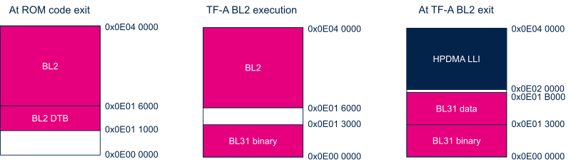
At runtime, the SYSRAM is split in two regions:
- 128kB Cortex-A35 Secure region dedicated to TF-A BL31 secure monitor.
- 128kB Cortex-A35 non-secure region dedicated to HPDMA linked lists management.
See SYSRAM internal memory for more information.
3.1.2. SRAM1 and SRAM2
In Cortex-A35 main processor mode, SRAM1 is used by FSBL TF-A BL2 to store DDR controller firmware and prepare OTP shadow.
At runtime, the first 4kByte of the SRAM1 are reserved for OTP shadow allowing to share OTP between Cortex-A35 OP-TEE secure OS and Cortex-M33 TF-M secure OS.
Rest of SRAM1 and SRAM2 are allocated in STM32MPU Embedded Software to Cortex-M33 secure and non-secure firmware, when not located in DDR for some low power or performance reasons.
The following figure shows the evolution of SRAM mapping during boot flow:

3.1.3. RETRAM
In STM32MPU Embedded Software, RETRAM is used for:
- DDR parameters saving to restore DDR access on low power modes exit.
- Cortex-M33 firmware that must be preserved in low power Standby mode. It is mainly the low power entry and exit functions executed by the Cortex-M33 secure context.

3.1.4. BKPSRAM
In STM32MPU Embedded Software, the BKPSRAM is used as following:
- 4kB dedicated to secure SW components context saving for restoration during low power exit sequence.
- 4kB for TF-M Internal Trusted Storage (ITS).

3.1.5. VDERAM
In STM32MPU Embedded Software, VDERAM is by default allocated to hardware video encoder and decoder if VENC or VDEC is assigned to one execution context.
Else if none is used, VDERAM could be allocated to any execution context.
3.1.6. LPSRAM
LPSRAM are dedicated to Cortex-M0+ firmware and associated shared memory. The default memory mapping is the following one:

Note LPSRAM are currently not used in STM32MPU Embedded Software.
4. DDR mapping
STM32MPU Embedded Software proposes a generic DDR mapping compliant with DDR from 256MByte to 4GByte, allowing to demonstrate all STM32MPU Embedded Software features.
The first 64MByte are reserved to firmware:
- Cortex-M33 secure OS (TF-M code and data)
- Cortex-M33 non-secure application (Cube code and data)
- Cortex-A35 secure OS (OP-TEE)
- Shared memory IPC between Cortex-A35 and Cortex-M33
Rest of the DDR is allocated to the Linux kernel and applications.
All bus master peripherals can access only to the lower 2GByte of DDR as they are 32bit capable. Linux CMA and reserved memories used for contiguous buffers allocation must be defined in the first 2GByte of DDR.
In case of generic memory allocation done in the higher 2GByte of DDR, Linux kernel offers SWIOTLB mechanism to recopy data in a bounce buffer located in the lower 2GByte of DDR compliant with 32bit bus master peripherals.
The following figure shows the evolution of the DDR mapping during the boot sequence.

It is customer responsibility to adapt DDR mapping to its product configuration (DDR size and SW components)
4.1. How to configure RAM mapping
The memory mapping is defined in each SW component device tree file using Reserved_memory bindings. Customer can change name, based address, size, and access rights of each region according to its product needs.
To ensure the consistency of the system, memory declarations of each SW component have to be updated according to the expected configuration.
ST recommends using CubeMX tools to generate coherent memory mapping with associated access rights.