1. What is a timer (TIM)?
The STM32 series devices have various built-in timers outlined as follows:
- General-purpose timers
- Advanced timers
- Basic timers
- Low-power timers
- High-resolution timers
This article will be focusing on the first three ones.
2. TIM with interrupt
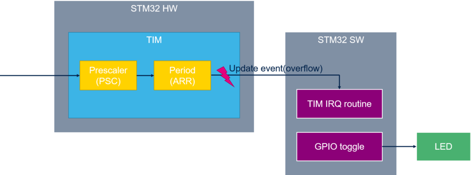
The STM32 families embed multiple timers providing timing resources for software or hardware tasks.
The software task consists mainly of providing time bases, timeout event generation, and time triggers.
The hardware tasks are related to I/O, timers can generate waveforms or outputs, and measure incoming signal parameters.
2.1. Objectives
The purpose of this example is to demonstrate how to:
- Configure a first TIM in CubeMX.
- Select timer frequency.
- Start TIM in code.
- Use TIM overflow(update) interrupt to toggle led.
2.2. Examples setup
To follow along with this wiki, a NUCLEO-L476RG board is needed.
Before starting the hands-on, make sure that the following software are installed:
STM32CubeMX 6.5.0 (or a newer version)
STM32CubeIDE 1.9.0 (or a newer version)
STM32CubeL4 firmware package
2.3. STM32CubeMX Timer configuration
- Run STM32CubeMX.
- Select Menu > File > New Project.
- Select NUCLEO-L476RG using the board selector.
- Start project.
2.3.1. GPIO configuration
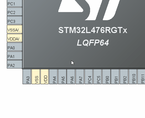
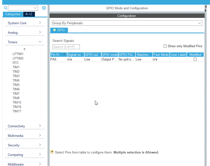
In the CubeMX Pinout view, select PA5 set as Output mode:
2.3.2. TIM configuration
2.3.2.1. Timer clock source selection
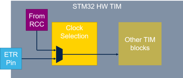
The timer features multiple clocking options. The default clock comes from the clock controller connected to one of the APB clock domains. The counter clock can be provided by the internal clock (RCC) or by the external clock through external trigger input (ETR pin), other on-chip timers (ITRx inputs), input pins (TI1, TI2), and quadrature signals from encoders.
In this example, the internal clock source is used. This information can be found in the product reference manual or datasheet.
The internal clock frequency is coming from the APB bus where the TIM is connected.
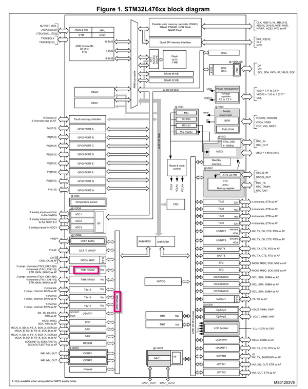
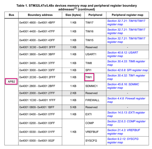
For example, TIM1 on STM32L476.
In the datasheet, it is possible to find the STM32L476xx block diagram where the TIM1 is on the APB2 bus.
In the reference manual, see System and Memory overview chapter to find a memory map where it is possible to find TIM1 on APB2.
For this application, the APB2 timer clock is 4 MHz.
2.3.2.2. TIM parameters configuration
In STM32CubeMX, select Timers => TIM1
- Select the Internal clock as the clock source.
2.3.2.3. Clock division
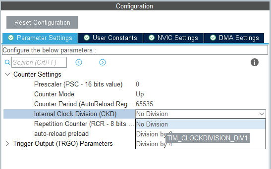
it is possible to divide the clocks by /1 /2 /4.
For this example, choose no Division(/1).
2.3.2.4. Clock prescaler
The prescaler can divide the counter clock frequency by any factor between 1 and 65536.
The counter clock frequency is equal to fck_PSC / (PSC+1).
In this example, APB2 clock = 4 MHz
No division in the clock division block (/1)
PSC input clock = 4 MHz.
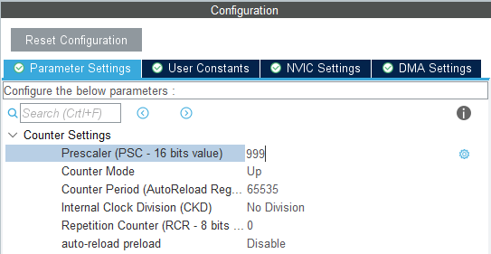
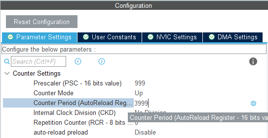
In order to divide it by 1000 (PSC+1)=> put PSC = 999.
Then have the output frequency from PSC 4 MHz/(999+1) = 4 KHz.
2.3.2.5. Counter period
This timer period:
For PSC = 999 and APB2 = 4MHz, with no division DIV = 1.
The input frequency is equal to 4 kHz.
To get the period 1s, set the ARR to 3999.
Where period is: f_out = APB2 / ( ARR + 1 ) = 4 kHz / ( 3999 + 1 ) = 1 Hz = 1s
2.3.2.6. Counter Mode
This counting mode is optional:
- Up: the counter counts from 0 to the auto-reload value (ARR).
- Down: the counter counts from auto-reload value (ARR) to 1.
- Center alignment(up/down): the counter counts from 0 to (ARR-1), then counts from ARR value down to 1. Then it starts counting from 0.
For further details, refer to section TIMx control register 1 (TIMx_CR1) in the reference manual.
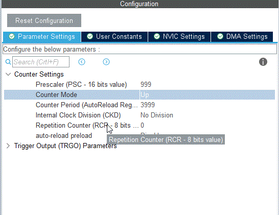
In this application example, choose the up-counting mode:
By now, the configuration should look like this:
2.3.2.7. Enable interrupt
The timer can have one or more interrupts. The basic one for timer overflow is called "update".
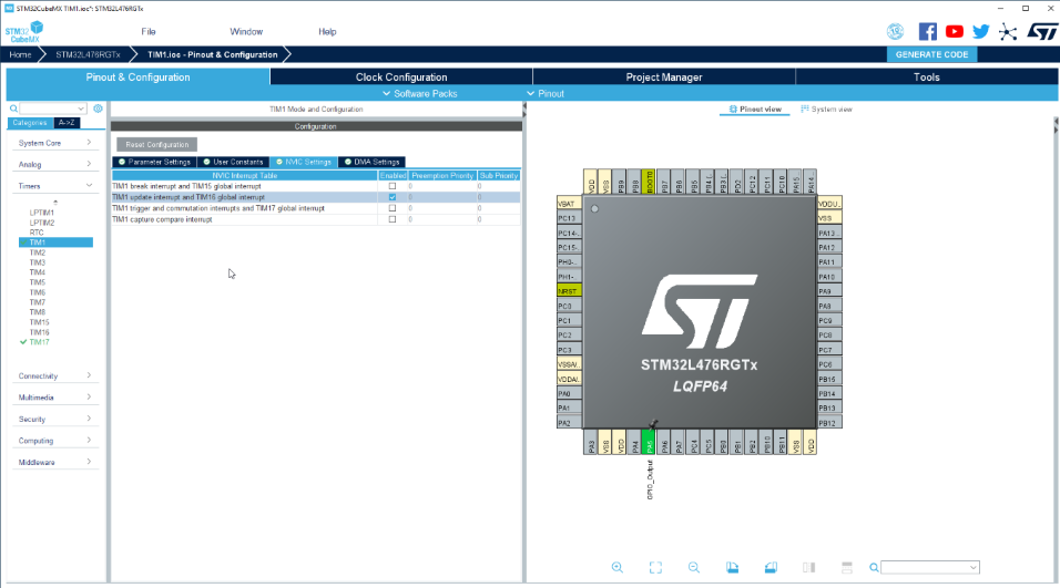
Switch to NVIC settings and select TIM1 update interrupt.
2.4. Code generation
- Go to Project Manager.
- Set the project name (TIM1).
- Project location.
- Type of toolchain (CubeIDE).
- Generate code.
2.4.1. Starting timer
The timer is now configured but not yet started.
For this, use the function: HAL_TIM_Base_Start_IT.
The first argument is the TIM1 handle htim1.
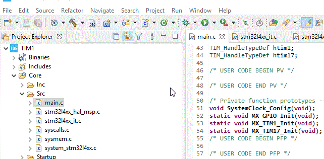
Between /* USER CODE BEGIN 2 */ and /* USER CODE END 2 */ tags, insert the function to start the timer:
  /* USER CODE BEGIN 2 */
  HAL_TIM_Base_Start_IT(&htim1);
  /* USER CODE END 2 */
2.4.2. Handling timer interrupt
When TIM1 interrupt is triggered, the function TIM1_UP_TIM16_IRQHandler is called. This calls the HAL library function HAL_TIM_IRQHandler which decodes the interrupt source. For this example, this function is only implemented to get the callback from the function HAL_TIM_PeriodElapsedCallback defined as __weak in stm32l4xx_hal_tim.c.
Redefine it in our main.c by adding a GPIO toggle: Between /* USER CODE BEGIN 0 */ and /* USER CODE END 0 */ tags, add:
/* USER CODE BEGIN 0 */
void HAL_TIM_PeriodElapsedCallback(TIM_HandleTypeDef *htim){
	HAL_GPIO_TogglePin(GPIOA, GPIO_PIN_5);
}
/* USER CODE END 0 */
2.4.3. Compile the code
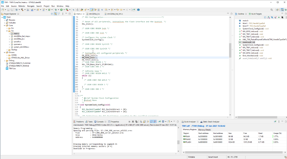
To compile project, press CTRL+B Or go to Menu>Project>Build all.
2.4.4. Run in debug
- Connect the board to the PC.
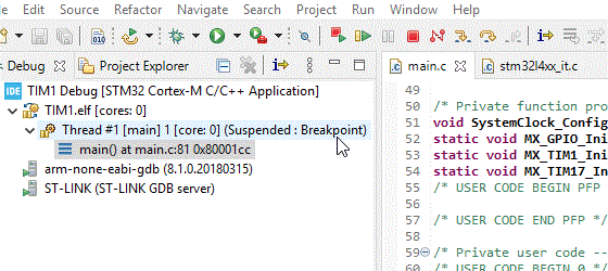
- Start debug.
- Menu>Run>Debug As>STM32 Cortex-M ...
- Click on debug without changing any option.
- Press F8 to run code.
The LD2 should toggle each second.
3. TIM with DMA transfer
3.1. Objectives
- Learn how to set up TIM with DMA in CubeMX.
- Indicate TIM DMA transfer with LED toggle.
3.2. STM32CubeMX configuration
This example will be based on the previous timer and GPIO configuration, except the step " Enable Interrupt" which will be skipped since DMA is used instead.
3.2.1. DMA configuration
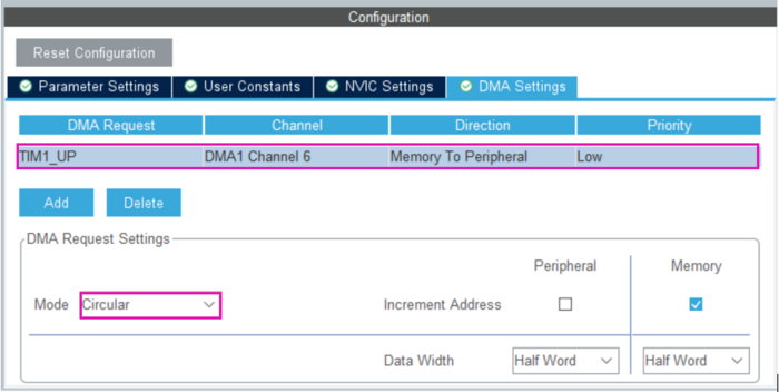
In the TIM1 configuration, click on "DMA settings".
- Add DMA request as TIM1 UP.
- Change direction to: Memory to Peripheral.
- Change DMA mode to circular.
3.3. Code configuration
The following flowchart describes the steps:
3.3.1. Variable data definition
Between /* USER CODE BEGIN PV */ and /* USER CODE END PV */ tags, add:
/* USER CODE BEGIN PV */
uint16_t data[]={GPIO_PIN_5,0x0000};
/* USER CODE END PV */
3.3.2. DMA and Timer start
Between /* USER CODE BEGIN 2 */ and /* USER CODE END 2 */ tags, add:
 __HAL_TIM_ENABLE_DMA(&htim1, TIM_DMA_UPDATE);
  HAL_DMA_Start(&hdma_tim1_up,(uint32_t)data,(uint32_t)&GPIOA->ODR,2);
  HAL_TIM_Base_Start(&htim1);
4. TIM synchronization
STM32xx Series timers are linked together internally for timer synchronization or chaining.
Each timer has several internal input and output triggers. These signals allow timer interconnection.
4.1. Objectives
- Explain timer internal triggering system.
- Use a master timer to start a slave timer: Trigger TIM2 with the update of TIM1.
4.2. STM32CubeMX configuration
Before configuring timers in STM32CubeMX, it is necessary to know which timer will start counting.
To do so, refer to the STM32L476 reference manual, internal trigger connections.
The table below shows how the timer triggers are connected internally. It is necessary to select the right timers for your application.
In this example, select TIM2 as a slave timer, and TIM1 as a master using ITR0 (TS = 000) internal signal.
4.2.1. Master TIM configuration
When a timer is selected as a master timer, the corresponding trigger output signal (TRG0) is used by the slave internal trigger (when configured).
The trigger output can be selected from the following list:
- Reset
- Enable
- Update
- OC1Ref
- OC2Ref
- OC3Ref
- OC4Ref
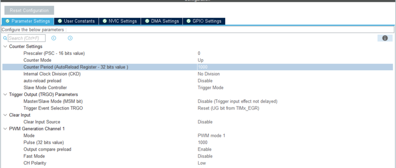
In this example, use the PWM output to monitor timer outputs.
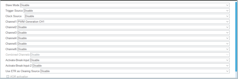
As TIM1 is the master timer, enable the PWM output on Channel1 only.
Use the same values of prescaler and Auto-reload as in the previous examples.
Choose the trigger event selection as an Update event: This will generate the update event flag whenever the counter overflows.
Set the Pulse to 800, as the Duty cycle = Pulse/ ARR, since ARR = 4000, choose Pulse = 1000 to obtain a 25% duty cycle.
Set the Channel polarity to low, in this case, the output will be inverted.
4.2.2. Slave TIM configuration
- Select the trigger mode as the slave mode.
- Select ITR0 as the trigger source.
Enable the PWM generation for TIM2 to visualize the output.
- Check that the slave mode controller is trigger mode.
- Set the channel polarity to LOW.
- Set the ARR value to a random value.
4.3. Code generation
In the main function, between /* USER CODE BEGIN 2 */ and /* USER CODE END 2*/ tags, add:
 /* USER CODE BEGIN 2 */
  HAL_TIM_PWM_Start(&htim1, TIM_CHANNEL_1);
  HAL_Delay(500);
  HAL_TIM_PWM_Start(&htim2, TIM_CHANNEL_1);
  /* USER CODE END 2 */
Add the delay between the two PWM starts to make sure that the slave mode is working, so the TIM2 won't start counting before TIM1.
After running the code, it's possible to use a logic analyzer to visualize the timer signals:
- TIM1_CH1: PA8
- TIM2_CH1: PA0
As shown in the image below, TIM2 starts after TIM1.
Note that there are several other modes used in timer synchronization. Refer to the examples provided in the
STM32Cube package:
Examples:
- \TIM\TIM_CascadeSynchro
- \TIM_ExtTriggerSynchro\TIM_Synchronization
- \TIM_ParallelSynchro folders
